Multi-channel programmable power control provides efficient DC rails
Today, systems place complicated demands on multiple low-voltage DC rails. Tuomas Hollman, Exar, explains how a power controller can manage diverse needs
The DC/DC power converter sub-systems in today's applications must support external control of many aspects of operation as programmed by the user. In designs with multiple supply rails, there is an increasing need for sophisticated management of the power conversion by a sophisticated controller IC and design tool, which will effectively support various converter combinations.
Programmable controllers for power conversion have been gaining in popularity. It can implement three to four complete, independent pulse-width-modulated (PWM) controllers, including a light load mode for low power dissipation and high efficiency at low output currents. It also must provide a number of critical safety features, such as over-current protection (OCP), over-voltage protection (OVP) and over-temperature protection (OTP) plus input under-voltage lockout (UVLO). A number of key health-monitoring features are needed, such as warning-level flags for the safety functions and a power good indication along with full monitoring of system voltages and currents. These functions are programmable and/or readable from an SMBus and many are steerable to the GPIO ports for hardware monitoring by the system controller. All housed in a small package for space efficiency.
Required features
The list of desired controller features is extensive and illustrates how much the design engineer expects the selected controller to do. The Exar XRP7724 quad-channel digital PWM/PFM programmable power management system (Figure 1) meets these requirements, says the company.
 Figure 1: Simplified schematic of XRP7724
It supports a wide switching frequency range, with independent, programmable channel-to-channel constant operating frequency. Each channel is configurable for soft-start and soft-stop sequencing, including delay and ramp control.
Another feature is its low standby/light load power consumption, with an ultrasonic mode to limit the audible noise emanating from inductor. Its integrated MOSFET drivers can drive a range of input gate-source capacitance values, while programmable five-coefficient PID control, with the output capacitor, allows the designer to finetune the control loop. The SMBus compliant-operations are fully controlled via an I2C interface. This allows for advanced local and/or remote reconfiguration, with full performance monitoring and reporting, as well as fault handling, says the company.
Controller architecture
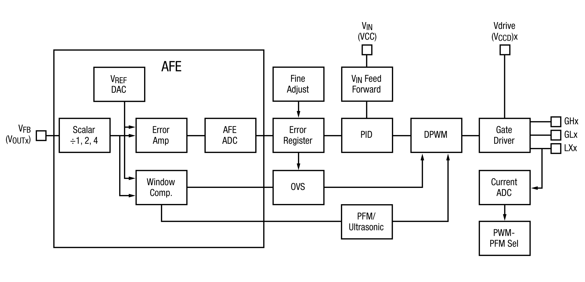
The functional block diagram of the regulation loops for an output channel (Figure 2), shows the four separate, parallel control loops, namely PWM, pulse frequency modulation (PFM), ultrasonic and oversampling. Each of these loops is fed by the analogue front end (AFE) at the left of the diagram. The AFE consist of an input voltage-scaling function, programmable voltage reference DAC, error amplifier and window comparator.
 Figure 2: The regulation loops shows the four separate, parallel control loops within the device
To provide current level information, the output inductor's current is measured by a differential amplifier that reads the voltage drop across the on-resistance (RDSON) of the lower MOSFET during its on time. This voltage is converted to a digital value by the current ADC block and the resulting current value is used to determine when PWM-to-PFM mode transitions should occur.
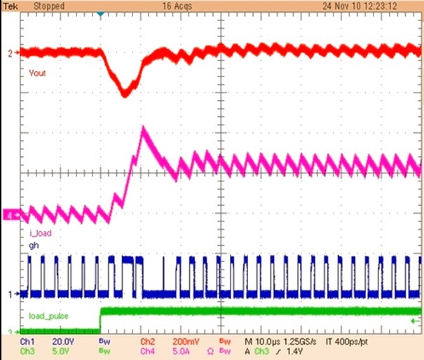
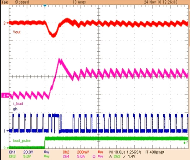
When powering CPU and digital-power modules, transient response is of the utmost importance (Figure 3 and Figure 4). That is where over-sampling mode is most effective, and was added to the XRP7724. In oversampling mode, the output voltage is sampled four times each switching cycle and is monitored by the AFE window comparator. If the voltage goes outside the set high or low limits, the oversampling control electronics can immediately modify the pulse width of the high-side or low-side gate drivers to respond accordingly without having to wait for the next cycle to start. Oversampling has two types of responses, depending on whether the high limit is exceeded during an unloading transient (over-voltage) or the low limit is exceeded during a loading transient (under-voltage).
PowerArchitect 5.0
In addition to a high-performance, function- and feature-rich IC, it is critical to have a user-friendly GUI (graphical user interface) to simplify fine tuning of the control-loop parameters for optimum performance.

Figure 3: The controller response for a 0A to 6A load transient, when operating at 300kHz in PWM mode only
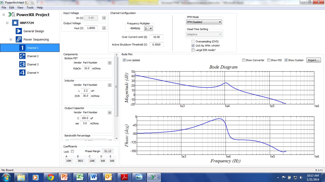
The PowerArchitect 5.0 design tool accelerates the selection of the powertrain components including output inductors and capacitors, as well as the control loop design. The tool generates a Bode plot based on the user's choices for the five programmable co-efficients of the proportional integral derivative (PID) control, as well the choice of switching frequency, output voltage and current. The user can either accept it or can modify the PID parameters to suit the requirements of the design.

Figure 4: The 10 to 6A transient response at 300kHz with oversampling at ±5.5%
The GUI screen (Figure 5) shows the selected switching frequency, output filter inductance and capacitance, PID co-efficients, Bode plot and phase margin, along with the control loop bandwidth for channel one. All of the related parameters are under the user’s control to finetune or even change completely for easy, immediate investigation of what-if? scenarios.

Figure 5: GUI of PowerArchitect 5.0
PWM- and PFM-mode control loops
The PWM control loop operates in voltage-control mode with optional input voltage feed forward. To obtain a full output voltage range, an input scaler is used to reduce the feedback voltage of higher output voltages, bringing them down to the reference voltage's control range. The error voltage is converted to a digital error term by the AFE ADC. The error register has a fine-adjust function that can be used to improve the output voltage's set-point resolution by a factor of five, resulting in low-, mid- and high-range resolution of 2.5, 5.0 and 10mV, respectively. The PID controller output uses the error resistor's voltage to manage the loop dynamics.
The controller has a PFM loop that can be enabled to improve efficiency at light loads. Reducing the switching frequency and operating in the discontinuous conduction mode (DCM) minimises both switching and conduction losses. The PFM loop works in conjunction with the PWM loop and is entered when the output current falls below a user-programmed threshold level for a programmed number of cycles. The PWM loop is disabled In PFM mode; instead, the scaled output voltage is compared to reference voltage using a window comparator.
In PFM mode, when the high-side FET is turned on, the inductor current ramps up and this charges the output capacitors and increases their voltage. After the completion of the high-side and low-side on-times, the lower FET is turned off to inhibit any reverse-current flow through the inductor. The load current then discharges the output capacitors until the output voltage falls below the reference voltage and the comparator is activated, which triggers the digital PWM function to start the next switching cycle. The time from the end of the switching cycle to the next trigger is referred to as the dead zone. This PFM technique ensures output-voltage ripple does not increase from PWM to PFM.
The switching duty cycle is the same as it was in PWM mode when PFM mode is entered initially. This causes the inductor's ripple current to be at the same level as it was in PWM mode. The PFM duty cycle is calculated based on the ratio of the output voltage to the input voltage. If the output voltage ever goes outside the high/low windows, the controller exits the PFM mode and reactivates the PWM loop.
Although the PFM mode improves efficiency at light load, the dead-zone time can increase at very light loads to the point where the switching frequency can be within the audio hearing range. When this happens, some components, such as the output inductor and ceramic capacitors, can emit audible noise. The amplitude of the noise depends mostly on the board design as well as the manufacture and construction details of the components. Proper selection of components can reduce the sound to very low levels. In general, ultrasonic mode is not used unless required, as it reduces efficiency at very light loads.


