Cascode Basics
A ‘cascode’ sounds like an archaic term from the era of vacuum tubes and that’s where it comes from. Cascodes today, though, are very relevant in their latest incarnation as combinations of SiC JFETs and Si MOSFETs, giving performance that’s getting very close to the suitable switch.
Guest blog by Zhongda Li, NPI Manager at UnitedSiC.
The ghost of Mr Miller
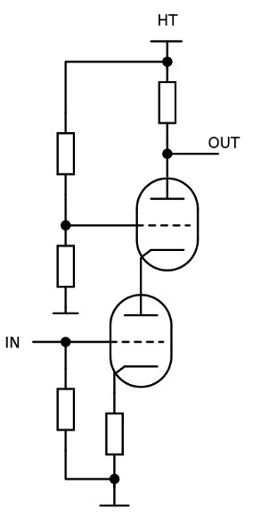
Back in the 1920s, the decorated US electrical engineer John Milton Miller, sometimes better known for his development of the ‘Miller’ crystal oscillator circuit, identified a problem with simple triode vacuum tubes used as amplifiers, due to the internal capacitance between the grid and anode. The effect reduced the bandwidth of the amplifier by imposing increasing negative feedback at higher frequencies with the reducing impedance of the capacitance. Miller’s eureka moment was to connect two triodes in a series arrangement (CASCaded triODE), or CASCODE (Figure 1), where the total capacitance from input to output is greatly reduced. The upper tube is controlled by its cathode being pulled up and down by the lower tube with the upper tube grid at a fixed voltage. When ‘tetrodes’ were developed with internal screens, the effect diminished, clearing the way for single tube amplifiers to operate into the hundreds of megahertz.

Figure 1. The original cascode
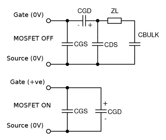
As semiconductors were developed, the effect re-surfaced, again restricting high frequency operation. The effect on modern MOSFETs used as switches is to limit switching speed, with the drive circuit having to cope with charging and discharging the input capacitance in a reliable and low-loss way. The effect of miller capacitance CGD varies, depending on the gate voltage; imagine an enhancement-mode MOSFET switch OFF with its gate at 0V. The total gate input capacitance appears as a network shown in Figure 2 including CGS, CGD, CDS, load ZL and bulk capacitance CBULK with a positive voltage across CGD. When the MOSFET is turned ON, the drain falls to near zero and the total capacitance is now just CGD in parallel with CGS with a negative voltage across CGD compared with the OFF state. In switching from ON to OFF and vice versa, the input capacitance swaps between these two conditions.

Figure 2. MOSFET equivalent input capacitance when OFF and ON
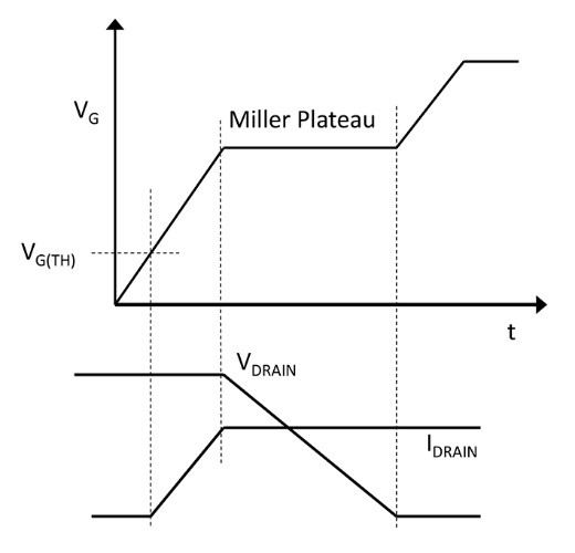
If you have ever looked at a MOSFET gate switching waveform, (Figure 3), that ‘plateau’ in the positive-going waveform is the transition between the two input capacitance states as the driver suddenly has to work harder, making the switching transition slower. Worse, as the drain drops in voltage, it tries to ‘push’ the gate negative through CGD, fighting the positive ON-voltage command. The reverse happens when driving the MOSFET OFF; CGD tries to ‘pull’ the gate positive, which is why a negative OFF-state gate voltage is often recommended with MOSFETs and IGBTs to try to counter the effect. This does increase gate drive power requirements, though.

Figure 3. Miller capacitance ‘plateau’ on gate drive voltage
CGD is a construction artefact
CGD is a feature of the physical construction of a semiconductor switch, so varies with lateral or vertical types. It can be designed to be low for low voltage MOSFETs but is a problem at high voltage, especially when designers want to use wide band-gap types using Silicon Carbide (SiC) or Gallium Nitride (GaN). The spectacular switching speeds promised by these technologies are still limited by what John Miller identified nearly a hundred years ago. His solution, though, is still the answer today.
Modern-day cascodes
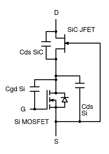
A basic Silicon Carbide switch is a junction FET or JFET. If it is fabricated in a vertical construction, CGD can be very low, which is what we need. Drain-source capacitance CDS is lower still. One little problem – a JFET is a normally-ON device with its gate at 0 V, needing a negative gate voltage to switch it OFF. This is not nice in a bridge circuit, when all devices default to ON at the instant of applying power. A normally-OFF device is what’s needed so the ghost of John Miller was invoked and a cascode arrangement of an Si MOSFET and SiC JFET was devised (Figure 4).

Figure 4. The SiC cascode
With the MOSFET gate and source at 0V, its drain rises in voltage. The JFET gate is also at 0V so when its source, the MOSFET drain, gets up to about 10V, the JFET has -10V gate-source and switches OFF. With the MOSFET gate positive, it is ON and the JFET gate-source is shorted, switching it ON. We now effectively have a normally-OFF device with 0 V on the MOSFET gate as we want. But look at the connections – the series input-output capacitance includes CDS for the JFET which is close to zero, so the spectre of Mr Miller and his effect are gone.
Bonus time
While switching, the Si MOSFET drain voltage is a ‘pot-down’ of the JFET drain voltage through the almost-zero CDS of the JFET and non-zero CDS of the MOSFET, so the MOSFET drain dynamically stays at a low voltage. This means that the MOSFET can be a low voltage type with very small RDS(ON) and non-critical gate drive. Better still, the body diode of low voltage MOSFETs can have a very low forward drop and fast recovery. The JFET has no body diode, so when third-quadrant, reverse-switch conduction is inevitable or necessary, such as in commutating bridge circuits or synchronous rectification, the MOSFET body diode conducts. This clamps the JFET gate-source to about +0.6V ensuring it is hard ON allowing reverse current to flow with low voltage drop.
Spectres banished
The SiC cascode solves the Miller capacitance problem in a neat way that also gives easy gate drive, normally OFF operation and a high-performance body diode. This is unlike SiC MOSFETs, with their poor body diode, or even GaN HEMTs, with lateral construction and high CDS. John Miller would be pleased that his effect has finally been laid to rest and he can now be remembered for his happier inventions.
More information about UnitedSiC and the benefits of using cascodes is available here.


