
The SiC semiconductor dream
Engineers have dreamed about the perfect semiconductor switch that has no conduction or switching losses, infinite voltage with no leakage and that is easy to drive. The dream continues, but the industry is getting pretty close with the latest SiC FET wide bandgap semiconductors
Wide bandgap (WBG) materials silicon carbide (SiC) and gallium nitride (GaN) have lower on resistance per unit die area and better electron saturation velocity than silicon and also have higher critical breakdown voltage per millimeter, leading to smaller chip sizes with resulting lower capacitances and higher potential switching speed. SiC also has much better thermal conductivity than silicon or GaN which, along with higher rated junction temperature, allows higher power dissipation from a given die and package (Figure 1).
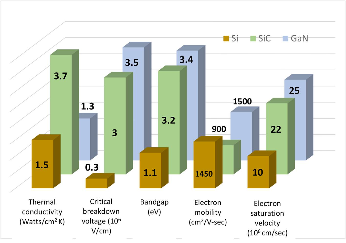
Figure 1: Material characteristics of silicon (Si), SiC and GaN
Challenges with WBG devices
WBG front-runners, SiC MOSFETs still have their challenges, with an inherently higher number of lattice defects than silicon, causing lower electron mobility and higher on-resistance. Gate threshold voltage also exhibits significant instability and hysteresis, while degradation of the gate oxide has been seen after stress events such as short circuits and over-voltage. An unexpected problem also occurred with ‘basal plane dislocations’ or bulk lattice defects which could grow and migrate, again increasing on-resistance and leakage current. There have been process improvements but manufacturers still rely heavily on defect screening during fabrication to keep field failure rate low. SiC MOSFETs also have particular gate drive requirements – to achieve lowest on-resistance, gate voltage must be close to the absolute maximum, so protection against over-voltage transients is important.
An alternative approach
SiC JFETs do not exhibit many of the MOSFET problems. JFETs are normally-on devices though, which is undesirable in practical circuits, so the idea of a ‘cascode’ has been revived. This is a combination of a high voltage SiC JFET and a low voltage co-packaged silicon MOSFET, or an SiC FET. The device is normally off, has all the WBG advantages, but has an easy, uncritical gate drive to the Si-MOSFET which, being a low voltage type, has a very robust gate oxide and low on-resistance.
The SiC JFET inherently has much better channel electron mobility than an SiC MOSFET. The channel is also shorter, so that for a given die area, SiC FET on-resistance is two to four times less or alternatively, up to four times the number of die can be obtained per wafer than with a SiC MOSFET for the same on resistance. Compared with a silicon superjunction MOSFET, the figure can be up to 13 times and the better performance helps to offset the higher material cost of SiC compared with silicon.
The gate of the SiC FET is that of the cascoded Si MOSFET. It has a stable, hysteresis-free threshold of around 5V and is therefore easy to drive to full enhancement with 12V or 15V, compatible with IGBT and Si MOSFET levels, with a large margin to the absolute maximum of typically 25V. Miller capacitance is effectively absent because of the small device dimensions and isolating effect of the Si MOSFET, so switching is very fast with low loss, with low output capacitance. In practice, edges will often be deliberately slowed to control EMI emissions and voltage overshoot, facilitated by an added gate resistor or a small RC snubber.
Third quadrant conduction
The diode in a SiC MOSFET has appreciable reverse recovery energy so dissipates some power and its forward voltage drop is high at around 4V. GaN HEMT cells conduct in reverse with no reverse recovery but again voltage drop is high and is related to the gate off-state voltage and channel resistance, resulting in a drop that can be several volts. The SiC FET exhibits a body diode with the characteristics of the low voltage cascoded Si MOSFET so its forward drop is around 1.5V and reverse recovery energy very low, about a third of a SiC MOSFET. The better performance of the SiC FET effectively opens up applications that Si MOSFETs cannot fulfil such as the fast switches in ‘totem pole’ power factor correction stages. Figure 2 shows the reverse recovery characteristics of a SiC FET and superjunction MOSFET compared for the same voltage class of device.
Enhanced reliability
The SiC FET has no SiC gate oxide and the gate of the cascode arrangement is that of a robust, low voltage Si MOSFET with high threshold voltage and thick oxide, protected by built-in zener clamps. SiC FETs have an avalanche rating, unlike GaN cells, and are inherently short circuit resistant with a channel ‘pinch-off’ effect which is consistent and independent of gate voltage, unlike MOSFETs and IGBTs.
Recent SiC FET introductions have silver sintering die-attach which yields a six-fold improvement in thermal conductivity of the interface compared with solder, keeping junction temperature rise low and reliability high.
SiC FET update
Since their introduction, SiC FETs have evolved. Rated voltages have increased and on resistance has decreased to the extent that the substrate is now the limiting factor and ‘wafer thinning’ is now employed to make further gains. Dynamic performance has improved so that the parts can be used with high efficiency in hard-switched topologies and at very high frequency is soft-switched operation as in LLC or phase shifted full bridge circuits.
Mounting options of SiC FETs have also expanded, from side-by-side co-packaged die in TO-247 and TO-220 packages to ‘stacked’ die arrangements. Leaded parts have been introduced with ‘Kelvin’ source connections to avoid problems with common inductance in the gate drive loop and more recently leadless DFN8x8 packages have been offered for lowest connection inductance and MHz switching.
UnitedSiC’s Peter Losee will take part in the WBG SiC: Serving Line Voltage and UP forum at PCIM 2021
About the author
Anup Bhalla is vice president of engineering, UnitedSiC

Featured products

MAX17793
Analog Devices Inc.

3V to 80V, 3A, High-Efficiency, Synchronous Step-Down DC-DC Converter
| SKU: | MAX17793 |
|---|---|
| Stock: | 9316 |
| Cost: | $3.64 |

MAX22516
Analog Devices Inc.

IO-Link Data Link Controller with Transceiver and Integrated DC-DC
| SKU: | MAX22516 |
|---|---|
| Stock: | 8000 |
| Cost: | $5.42 |
Product Spotlight
102991834
BeagleBoard

Single Board Computer (SBC), BeagleY-AI
AM67A BeagleY-AI Jacinto 7 AR...
| SKU: | 2820-102991834-ND |
|---|---|
| Stock: | 212 |
| Cost: | $56.24 |
SC1110
Raspberry Pi

Raspberry Pi 5 2GB
The Raspberry Pi 5 2GB model represents a leap for...
| SKU: | 2648-SC1110-ND |
|---|---|
| Stock: | 0 |
| Cost: | $38.33 |
AKX00069
Arduino

Arduino Plug and Make Kit
The Arduino Plug and Make Kit features the ...
| SKU: | |
|---|---|
| Stock: | 968 |
| Cost: | $66.97 |
300361-0011
Molex

MX150 Mid-Voltage MatSealed Female Connector Assembly, Dual Row, 20 Circ...
| SKU: | |
|---|---|
| Stock: | 280 |
| Cost: | $2.51 |