Packaging improves thermal performance
The SOT-223 package allows for a 10% cost reduction, in comparison to DPAK, writes Rene Mente, Infineon Technologies. The SOT-223 is a direct pin-to-pin replacement for DPAK designs with slightly reduced thermal behaviour in comparison to DPAK.
The SOT-223 pin-to-pin replacement for DPAK designs is the first SOT-223 package available without a middle pin, using the company’s CoolMOS CE series featuring up to 700V breakdown voltage (V(BR)DSS).
The strategy is to use SOT-223 on the existing DPAK footprint and allow slightly higher mould compound temperature. It is recommended to allocate additional copper area in order to reduce the overall Rth,JA (thermal resistance from junction to ambient). With 100mm² copper area on the drain pin available, the mould compound temperature will be approximately 2.0 to 3°C higher if SOT-223 is used instead of DPAK.
 Figure 1: Comparison of SOT-223 and DPAK packages
Figure 1 shows the middle pin has been omitted in the SOT-223 design. This offers an advantage with respect to soldering processes. During wave soldering solder residues between gate/drain and drain/source can occur, and in some cases it may also resist the cleaning process. The residues could cause arcing during operation and lead to destruction of the whole application if the over-current protection is not fast enough. The package design increases the distance between low voltage and high voltage pins resulting in a reduction of this possible failure.
Thermal simulation
Since the overall Rth,JA is responsible for the thermal steady state behaviour during operation the Rth,JC (thermal resistance from junction to case) is not relevant for SMD devices. The overall Rth,JA can be influenced by the copper and its thickness used on the PCB. Figure 2 represents the simulated junction temperature difference of SOT-223 and DPAK for the same chip with the attachment on different copper areas. The copper thickness is defined with 35µm (typical for low power designs), with 250mW losses of the MOSFET and an ambient temperature of 70°C.
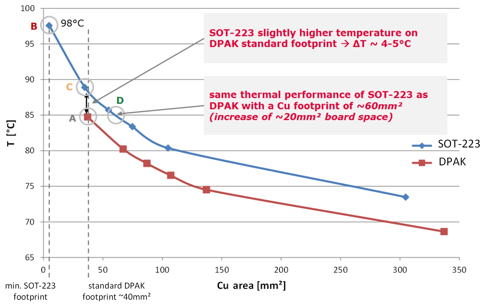
Figure 2: Thermal simulation of junction temperature at 250mW and ambient temperature of 70°C
Figure 2 shows four points (A, B, C and D), described in Table 1. It also reveals that for a direct replacement at 100mm² available copper area (and higher) the thermal difference between DPAK and SOT-223 is in the range of 4°C.
|
A |
DPAK on DPAK footprint ~40 mm² copper area |
This point represents the minimum copper area which is given due to the recommended minimum pad dimensions for DPAK package. It is clearly visible that under the mentioned conditions the junction temperature is simulated to be 84°C. This is used as reference. |
84 °C |
|
B |
SOT-223 on SOT-223 footprint ~10 mm² copper area |
The implementation of SOT-223 on the minimum footprint adds additional 14 °C junction temperature in comparison to DPAK. This setup can be used for low power levels, board space savings are possible. |
+14 °C |
|
C |
SOT-223 on DPAK footprint ~40 mm² copper area |
Accepting 5 °C higher junction temperature, this setup allows for a direct drop-in replacement for DPAK. This can be acceptable for DPAK designs with 5°C margin to thermal specification limits. |
+5 °C |
|
D |
SOT-223 on DPAK footprint plus additional copper area ~60 mm² copper area |
Applying ~20 mm² more copper area to the drain pin than the standard DPAK minimum footprint the thermal disadvantage of SOT-223 is eliminated. |
equal to DPAK |
These findings from a thermal simulation are now being checked against a real application measurement.
Let us consider the thermal behavior of the SOT-223 package in a 110W LED driver which makes use of the ICL5102 controller from Infineon Technologies.
Application measurement
As it is not possible to measure the junction temperature the following temperatures always represent the maximum mould compound temperature.
Typically, DPAK packages are used in the PFC and LLC stage of a 110W LED driver. In this case it is feasible to implement the IPN50R650CE, packaged in SOT-223, instead of in the LLC stage. The PFC stage uses a much lower RDS(ON) class which is not currently available in SOT-223. This design also benefits from the fact that a copper area in the range of 300mm2 is available on the drain connection. In approximately 90% of comparable DPAK designs, a copper area of more than 100mm² is already available.

Figure 3: SOT-223 in LLC stage of 110W LED driver
It can be expected that a replacement will lead to a temperature increase of no more than 4°C, depending on the overall power losses generated by the MOSFET. The thermal measurement (Figure 3) shows a temperature difference in a worst case scenario of 2°C normalised to 25°C ambient temperature when IPN50R650CE in SOT-223 is compared to IPD50R650CE in DPAK
Therefore the SOT-223 package can be a direct replacement for DPAK on minimum DPAK footprint if a 5°C higher junction temperature is acceptable. If the copper area connected on the drain pin is approximately 20mm² larger than a DPAK footprint, the SOT-223 will have the same thermal performance as DPAK on minimum footprint. If the available copper area is larger than 100mm² the SOT-223 can be a direct replacement for DPAK when accepting a 2.0 to 3°C higher temperature.
Infineon: PCIM Hall 9 – 412


