Package progress for high current densities
The first packages for power semiconductors were very large, difficult to process and a challenge to cool well. Infineon has created the TO-Leadless power package for high-current applications. Ralf Walter, Infineon Technologies explains.
Following the introduction of the PCB, it was possible to contact components without the need for wiring. This made it possible to take advantage of through hole technology for power semiconductors. As a result, a large number of cooling-optimised package shapes like TO-247 and TO-220 were developed. For various system requirements, SuperSO8 and CanPAK packages were developed; the latter is particularly well-suited for topside cooling.
Selection options
For a long period of time, no significant progress was made on surface mount semiconductor packages for large chip areas. The D²PAK received four additional source leads as well as one additional internal bond wire, and became D²PAK 7pin. It was the package of choice for applications that require high currents and low package resistance.
In addition to package resistance, several other characteristics are important when choosing a package and should also be considered when selecting components, such as component parameters such as mechanical dimensions and parasitic inductance. An electronic component must also be consistently solderable and have a very long operating life, even under harsh conditions.
Package resistance
The standard D²PAK, based on TO-220 with approximately 1mΩ, has a package resistance of less than 0.7mΩ; D²PAK 7pin is only about 0.4mΩ. This can be taken even further with modern trench technology in the low blocking voltage range, where maximum forward resistance in the range of one mΩ or less can be achieved very easily. The low package resistance afforded by D²PAK 7pin (0.4mΩ) accounts for a major proportion of the total resistance and cannot be ignored.
With regard to the overall electrical pathway of a typical power semiconductor package from drain to source, the total resistance is comprised of the silicon, copper lead frame (mostly drain contact), chip metallisation, bond wires (or copper clip or similar) and leads.
Component parts
The copper lead frame has negligible resistance, the thickness and type of chip metallisation is determined mostly by the technology. Its electrical resistance is also very small. Together they account for less than 20% of the total package resistance.
The electrical resistance of the bond wires can be reduced in various ways. The simplest method is to increase the number of wires and enlarge the diameter, although for mechanical reasons there are limitations. Theoretically, a more conductive material could be used if it were not for the prohibitive cost and difficulty of processing those materials. Much more can be achieved by reducing the length of the bond wires.
If the external lead contact area is also improved, electrical resistance is reduced significantly and values of less than 0.25mΩ for the entire package can be achieved. The TO-Leadless package has no external leads and up to five internal bond wires that were reduced to a minimum length. The five bond wires are connected to the chip metallisation across a large surface. The thin gate bond wire is contacted at the small square to the left.
Operation
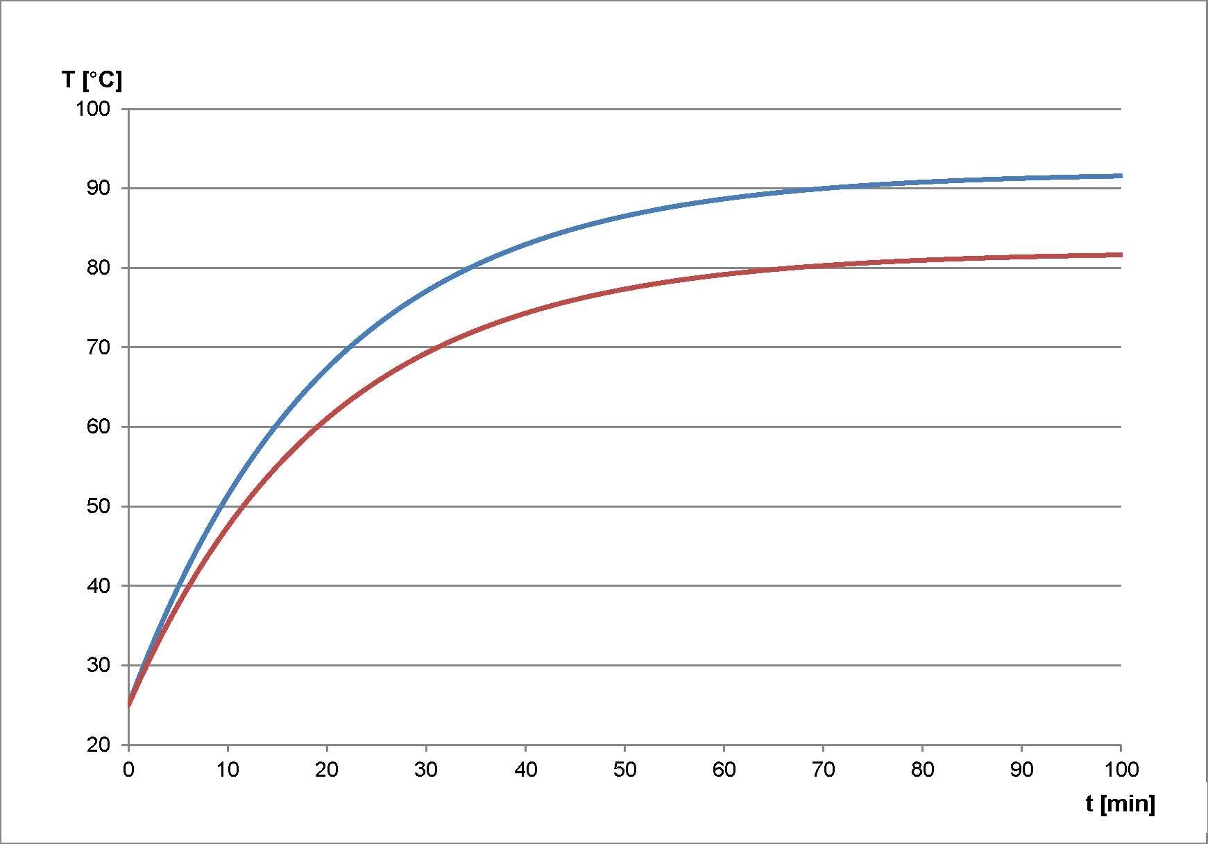
The practical benefit of this was tested in a typical motor control application. This test compared the high-current packages D²PAK 7pin and the TO-Leadless. The MOSFETs have identical chip surface (30mm²) and the same silicon technology (60V OptiMOS 5). The only difference is the package. These ensure respective maximum values of 1mΩ for the MOSFET in D²PAK 7pin (IPB010N06N) and 0.75mΩ for the MOSFET in the TO-Leadless package (IPT007N06N).
After 100 minutes the temperature difference is greater than 10°C (Figure 1). The lower losses and the associated lower chip temperatures simplify thermal management and help increase operating life.

Figure 1: Temperature progression in three-phase motor control electronics (10kHz, 24VDC, 100A)
Particularly in motor applications, operating life is very important. The development of electronic components is accompanied by a series of tests that examine reliability. Temperature plays a large role in these tests. Generally speaking, the absolute temperature values do not cause the greatest stress on the components. Instead, it is the change in temperature that is important. Typical power semiconductors are constructed from a variety of materials which, naturally, have different thermal expansion co-efficients. As additional components are added, the soldering and the board play a role as well.
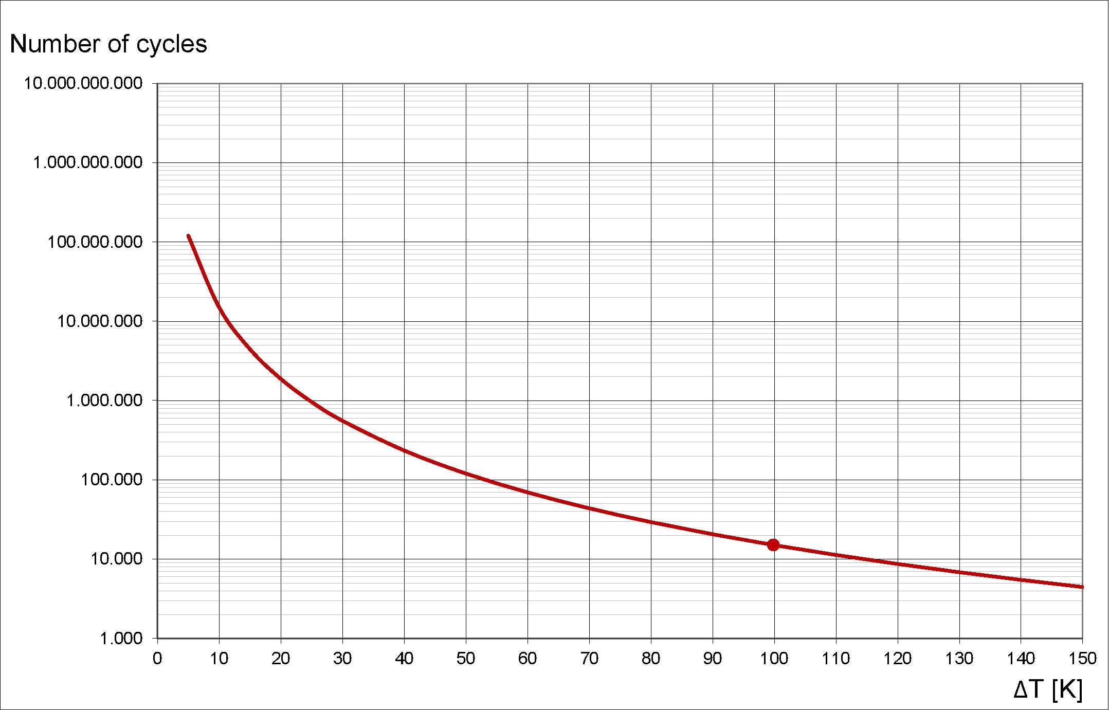
Another important test is the Intermittent Operating Lifetime Test, also known as power cycling. Following the guidelines of standard AEC Q101, the component is heated up internally over a short period of time using its own power dissipation and then cooled back down through simple convection. The component passes the test if it withstands 15,000 cycles without destruction or drift of its electrical parameters. Although the test produces only one measuring point (Figure 2, measuring point in the diagram at x = 100K, y = 15,000 cycles), it is still possible to calculate the minimum anticipated number of cycles at other temperature swings as well. This produces a cycle stability curve across a wide range of temperature swings.

Figure 2: IOL test. Measuring points and number of cycles calculated according to AEC Q101
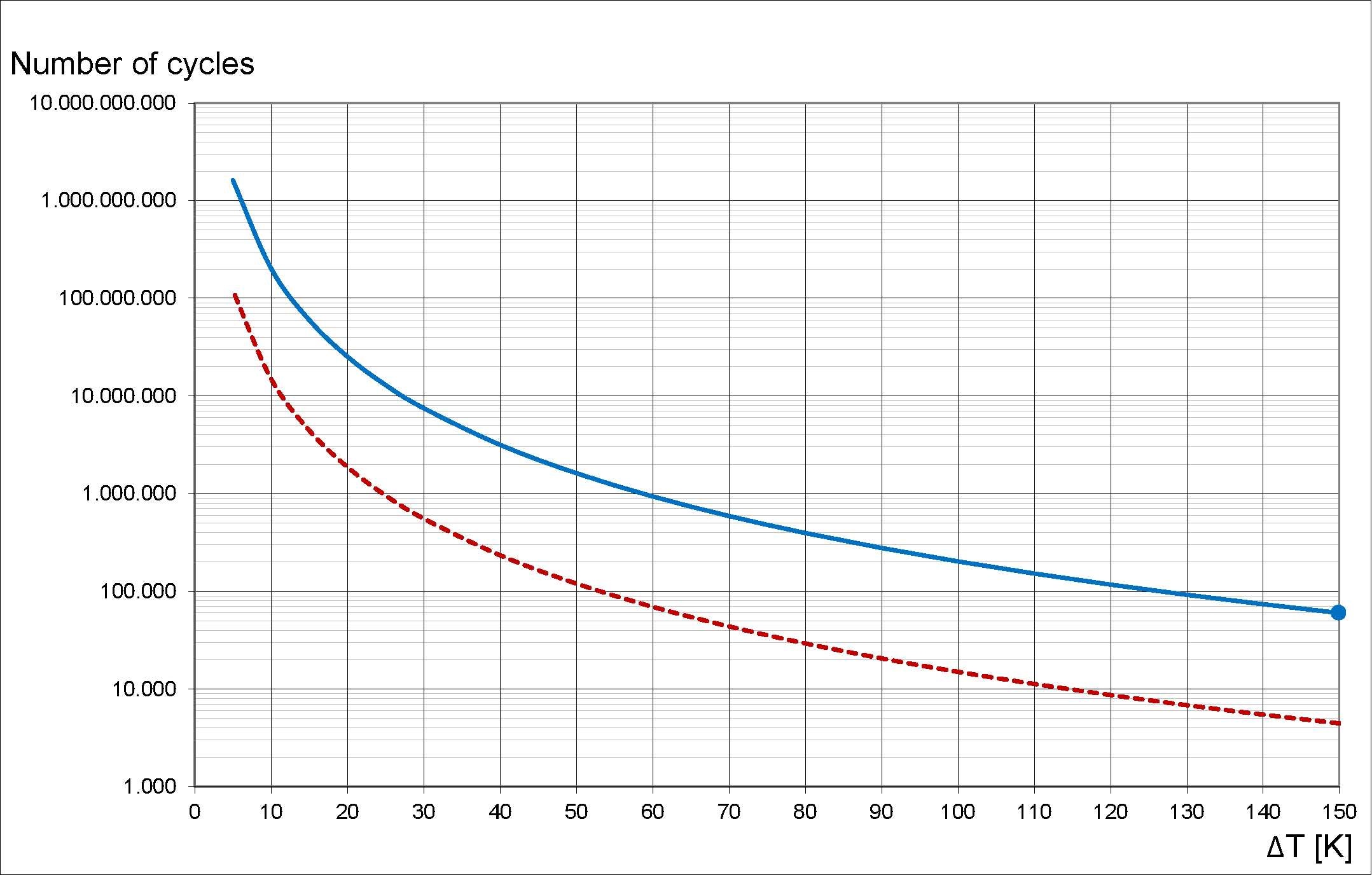
Instead of increasing the temperature by 100k, the power MOSFET in the TO-Leadless package was subjected to a temperature increase of 150k. Figure 2 shows reaching fewer than 5000 cycles (instead of the 15,000 at ∆T = 100K) would be an acceptable value. The TO-Leadless package withstood a significantly greater number of temperature increases. Even after 60,000 cycles, there was no detectable drift of the electrical parameters (Figure 3). Convert this to the temperature increase demanded by the standard (∆T = 100k) to realise an anticipated cycle stability of 200,000, which is more than 13 times the requirement of the standard.

Figure 3: IOL test (blue curve) with TO-Leadless with ∆T = 150K and calculated cycle stability curve in comparison to IOL according to AEC Q101 (red dotted curve).
Optical inspection
Reliability also depends on how the component is soldered onto the board. With power semiconductors such as D²PAK, evaluation is straightforward, requiring only AOI, which is available at most board manufacturers.
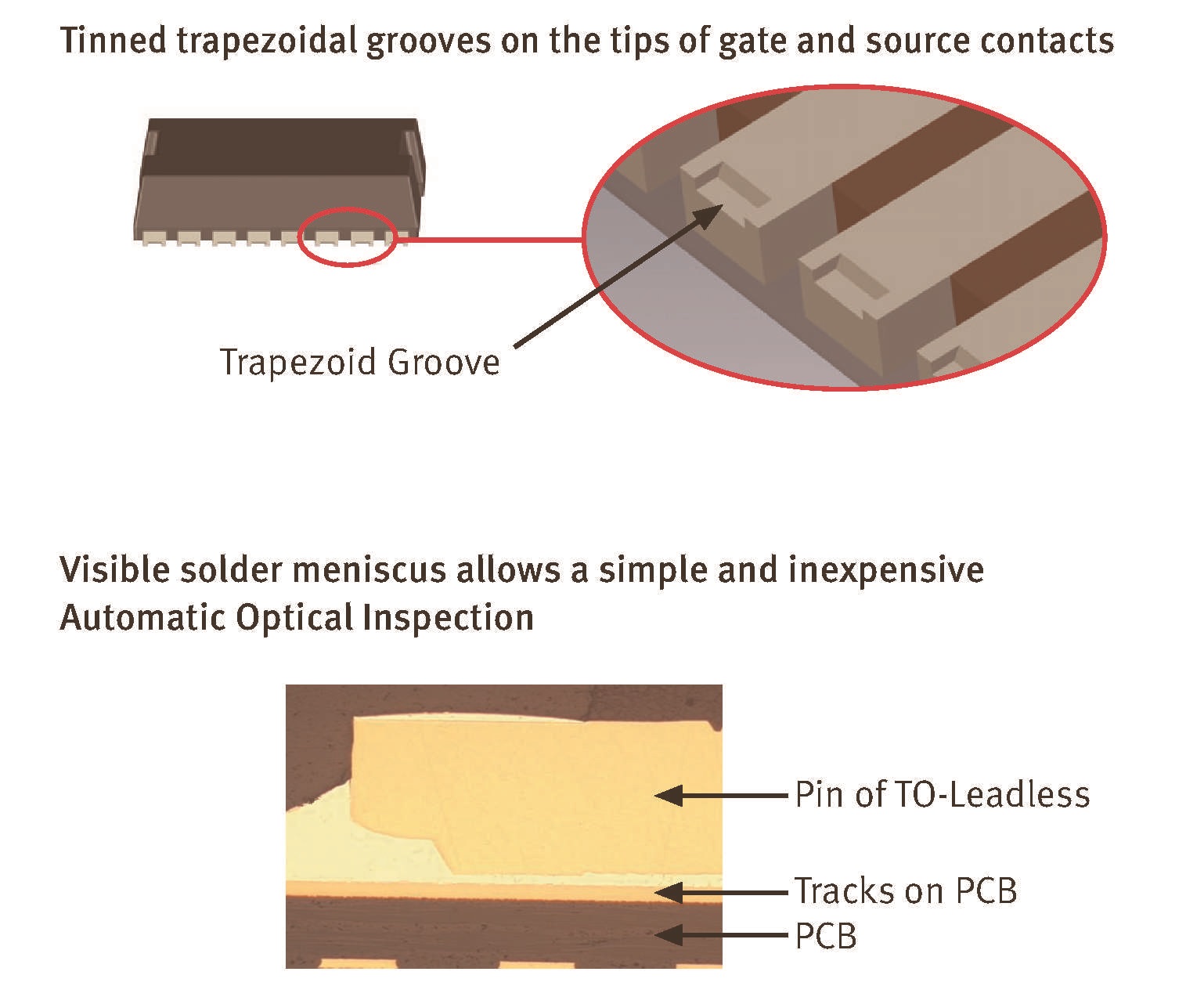
Although a TO-Leadless package does not have significantly protruding leads, solder quality can be evaluated using the normal AOI process. In the three-dimensional and rotated views, the exposed (copper) cut surface and the tinned crimp are readily identifiable. The soldering results are seen on the highly enlarged cross section to the right. The solder is light in colour, the source lead pin is dark with the impressed crimp. At the left edge of the image there is the beginning of the solder meniscus that is also visible externally (Figure 4).

Figure 4: View of the tinned trapezoidal crimp at the gate and source leads (above). Results of the solder process are seen below: The visible solder meniscus permits straightforward and economical AOI
The development of the TO-Leadless package has made it possible to fulfill the requirements of applications with high currents and reliability. The low package resistance reduces losses and makes thermal management easier. The ability to utilise optical inspection also reduces costs and permits reliable assessment of the solder connection. The result is a power package that permits high current density in a small area without compromising reliability of the assembly.
PCIM 2015 Hall 9 - 412


