Mobile battery life vs Moore’s law – a survival guide
The end of Moore’s law has been signaled for some time, but without a doubling of the number of transistors, battery-powered mobile devices rely on it to increase computing complexity. Gordon Allan offers a survival guide to life outside Moore’s law
For some years now the semiconductor industry has acknowledged a looming discontinuity — the slowing down and eventual end of the historical trend projected by Moore’s Law: the doubling of transistors on ICs every two years. Yet highly integrated, battery-powered mobile device applications depend on this trend’s continuation to deliver low power with increased compute complexity. The demise of Moore’s Law threatens these applications.
As the growth in the number of transistors per IC slows, lowering power consumption at the MOSFET transistor level has faded in importance as a driver of design innovation. Therefore, because mobile apps will continue to require more and more complexity, lowering power consumption will have to come from other sources. This realignment is already occurring in force.
When looking at the nature of the threats this poses to mobile applications, and how the design community is fighting to survive them, there are several developments in this evolution to consider. Some have just begun, others are reaching maturity, and many will stand for several more years as “plans of record” and as requirements for participating in current and future mobile phone and tablet markets. Factors include SoC and processor architectures, EDA contributions, software verification strategies, client / server / cloud relationships and memory storage technologies. These are all elements in a survival guide for succeeding in the post-Moore’s law future.
Shortlist for survival
The SoC architecture revolution has already happened. Multiple cores and coherent cache architectures allow several variants of performance profiles for an application, including parallelism with fine control over power, speed on-tap when required and dormant when not, and always-on, low level functionality with minimum current draw. This means that multi-core is the norm in the handheld device as well as the server farm.
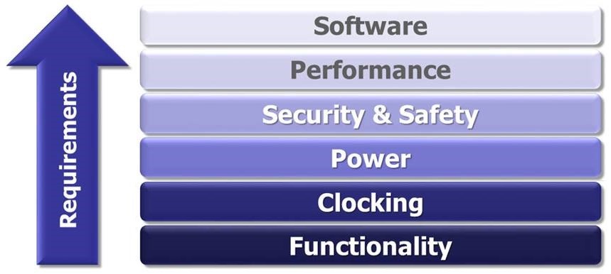
Thus, the distinction between mobile compute power and server compute power in architectural terms has diminished. This development has been furthered by on-chip bus protocols and advanced cache algorithms, which have ranked power consumption as a primary design consideration along with functionality and performance / throughput for many years.
Von Neumann architectures are still the CPU of choice for most SoC control and system logic and for most application software. We are, however, seeing greater use of other processor architectures, such as neuromorphic, where the power / performance ratio is an advantage - for example, detecting and predicting patterns in complex data. Applications that detect and predict these patterns are the stars of critical mobile solutions such as speech and face recognition in particular and assistive applications in general. These apps require a device to adjust and interact to a world in constant flux and include any app that is always-on.

New requirements drive increasing complexity
Available tools
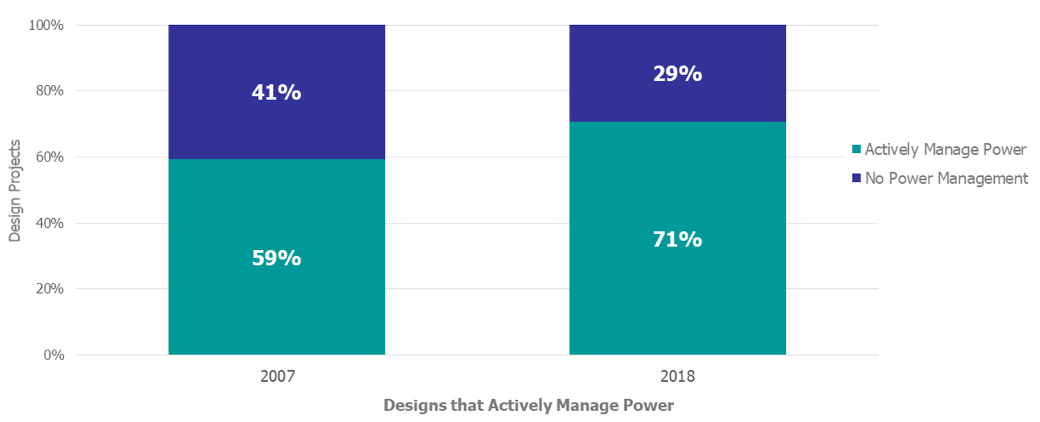
What about the tools available to designers? SoC designs need increasingly complex low power architectures and features. To enable ease of low power design, one area of focus for EDA companies has been in capturing and codifying low power into the IEEE Standard 1801 unified power format (UPF). The UPF supplies every mobile SoC designer with the consistent, high quality, low power constructs required for designing and verifying multiple clock domains, power domains, and power / voltage islands on-chip. The 2018 Wilson Research Group Survey commissioned by Siemens EDA, found that 71% of designs actively manage power, up from 59% a decade ago. That number is closer to 80% for large ASICs.
There is a lot of complexity that needs to be designed and verified, and the UPF standard, along with the EDA simulation, debug, and analysis tools that support the standard, bring the complexity problem down to size. According to the Wilson Research Group Survey, it is one of the more successful standards in terms of adoption, with respondents reporting UPF 3.x as the plan of record for many new designs.
A second wave of low power design and verification solutions have already been introduced by EDA companies. These include analysis tools that recommend or insert power reduction logic on constructs that are identified during simulation as good candidates for optimization. We predict future on-silicon monitoring to gather usage data on power-hungry design constructs so designers of subsequent iterations can have all the data they need to make further optimisations. Each and every designer is part of the team, prolonging the effects of Moore’s law beyond mere transistors.

IC/ASIC power management. (Source: Wilson Research Group and Siemens EDA, 2018 Functional Verification Study)
System verification
The system / software part of a design is an important part of the survival kit. One area that is increasing in importance in SoC verification over the last 10 years is the need to verify the firmware and application software parts of an algorithm. Sometimes that requires more extended testing than simulation can deliver, calling on emulation and emulator low power apps. These incorporate the firmware and operating system parts of the algorithm directly into SoC verification rather than merely mimicking them, possibly incompletely, in a simulation testbench.
In the wider software sphere, applications and mobile operating systems are playing a greater role in minimising power usage. In the so-called app economy, products will often succeed or fail depending on their impact on battery life.
The cloud is an important character in this survival guide. One shift in mobile electronics that has been in part driven by low power considerations is client / server computing. Multiple generations of improvements in cellular networks and Wi-Fi networks have enabled this shift and continue to do so. For example, 5G cellular networks have an energy efficiency benefit of 1000x in bits per Joule. This makes the use of cloud applications on mobile phones and tablets very inviting.
One technology area that has already matured in its adaptation for low power, on the back of the high density requirements, is memory storage. In recent years there has been a move from active storage technologies and rotating magnetic storage to static technologies at scale, such as flash memory. NAND flash is used for highest density, and NOR flash can be used for a slight power consumption benefit, especially if the flash data is read-mostly. Flash is one part of the illusion of an always-powered-up mobile device.
In semiconductor technology, there are other technologies waiting in the wings. These can include new materials and transistor structures for semiconductors as alternatives to traditional MOSFETs, such as Indium Gallium Arsenide based, graphene based, quantum well, and tunnel-effect transistors, as well as tomorrow’s optical and quantum computing technologies. Some of those may succeed. When the economics are right, the industry will pick the solution for the challenges of the day. Other technological advances include the miniaturisation of discrete sensors, such as accelerometers and gyroscopic position / movement sensors. These are a significant growth area in the industry right now.
Surviving in the new era
A low power survival guide contains many techniques and areas of defence, for example SoC / CPU architectures, storage, ease of low power design, ease of verification, well-designed software and firmware, and the effects of the cloud and the communication capabilities of tomorrow. All of these are equally important to continue the legacy of Moore’s law as an expression of complexity of technology and the impact of that technology on our daily lives. With these survival skills in hand, designers of mobile and tablet technologies can adapt for survival for years to come.
About the author:
Gordon Allan is the Questa Verification IP product manager at Siemens EDA. He was one of the architects and developers of Accellera UVM and has worked in SoC design and verification in lead engineer and senior consultant roles


