Automating product development - from design through to manufacture and test
Increasing design automation requires an appreciation for the challenges incurred and complexities involved at every stage of product development. EDA tools targeting complete product design offer many benefits, including the ability to increase functionality through extensions and plug-ins. Robert Huxel, Technical Marketing Manager, Altium and Philip Ling, Technical Marketing Manager, XJTAG explain.
As the sophistication of electronic products increases, the complexity involved with their design also escalates. Design tools must evolve to keep pace with the demand for greater automation, without restricting creativity.
Automating even part of the engineering process is an effective way of addressing both the cost and complexity of product design. Given that the electronic design automation (EDA) industry is estimated to be worth around $7bn, it is clear EDA tools are now essential in minimising the cost and complexity of electronic product design.
The design, manufacture and test of PCBs fundamentally underpins product development and while each stage flows into the next, PCB design drives the entire process. The application of EDA tools at the schematic capture and PCB layout stages of design can bring major benefits, and now those benefits extend beyond design, to include the stages of manufacture and test.
Making manufacturing simpler
Moving from schematic capture to PCB layout and design within a single environment offers many benefits in terms of design automation. Having the data available natively means all aspects of design can be more closely coordinated. As the industry’s leading example of a unified design environment, Altium Designer was conceived to bring together all aspects of product design.
This is evident in the seamless way it enables engineering teams to begin a design in the 2D world of schematic capture, then move to the design of rigid and flexible PCBs using 2D and 3D visualisation. Using Altium Designer, this flow can continue through to the mechanical design of enclosures using advanced 3D views, all within the same environment. This advanced capability also allows design decisions to propagate between all domains.
Forming a flexible PCB to fit inside an enclosure, measuring the proximity of components near to a heat sink, or positioning a chassis fixing so it is accessible after final assembly, are all significant design considerations. These involve decisions that are best made before sending the design out for manufacture - and using Altium Designer they can be.
Of course, all of these design decisions still need to be documented before manufacturing can begin. Now, the latest version of Altium Designer, version 16.1, adds a further dimension to the support it offers to the manufacturing process. It introduces a feature called Draftsman, which brings a greater level of automation to the process of documenting a design.
Using Draftsman, all the data entered during design can be used to automate the process of generating the documentation needed for manufacturing. Furthermore, because it exists within the same unified environment, any design changes that impact the manufacturing process are also automatically reflected in the documentation, saving many hours of effort. By removing the need to manually update the documentation, engineering drawings are always up to date and always ready to use.
Figure 1 (pictured above): Draftsman allows designers to intelligently automate the process of generating the necessary documentation for manufacturing
Tackling test challenges
Following design and manufacture, inevitably, comes test. Historically, EDA tools have not addressed the process of test explicitly, but have instead focused on the design elements of testing - normally referred to as Design For Test (DFT). This extends to manufacturing, with Design For Manufacture (DFM) playing an equally important part in overall product design.
While design constraints can be used successfully in EDA tools to help promote good DFM practices, design automation at this level has been largely confined to PCB layout or enclosure design, where user defined constraints can be used to automatically check the physical proximity of components, for example. Implementing design automation at the schematic capture stage requires a different approach.

Through its ability to accept Third Party extensions, Altium Designer now offers a feature that can automatically verify a design, at the schematic capture stage, for its testability using Boundary Scan. Boundary Scan (also known as JTAG) is the preeminent technology used for testing PCBs with limited physical access. It requires just a simple 4-pin interface to electrically access multiple points on a PCB and, as such, is the most common way of testing PCBs that feature Ball Grid Array (BGA) or Land Grid Array (LGA) packaged devices. However, it is also used extensively for debugging and in-system programming (ISP), making Boundary Scan applicable in any PCB, of any complexity, featuring any type of component package.
As an IEEE Standard, Boundary Scan first appeared in 1990 to address the need for testing connections between pads on flip-chip packages, where direct physical access is restricted. Today, it is essentially a free technology, because semiconductor manufacturers include it ‘by default’ in a wide array of ICs. Making use of this free technology simply requires selecting JTAG enabled components, adopting a DFT approach to design, and having access to test equipment designed to support Boundary Scan.
While Automated Test Equipment (ATE), including Flying Probe and In-Circuit Testers, do support some Boundary Scan functionality, it is dedicated Boundary Scan systems like the products developed by XJTAG that really provide full support for all its features and capabilities.
Now, for the first time, a PCB design tool automates the verification of Boundary Scan design during schematic capture. Available free of charge to all Altium Designer licensees, an extension called XJTAG DFT Assistant for Altium Designer offers DFT features that can deliver significant benefits in designs of any complexity. Developed by XJTAG specifically to support the design and verification of Boundary Scan Chains, it automates a process that would otherwise need to be carried out manually. Crucially, it also provides guidance on resolving design problems that could inhibit Boundary Scan from working.
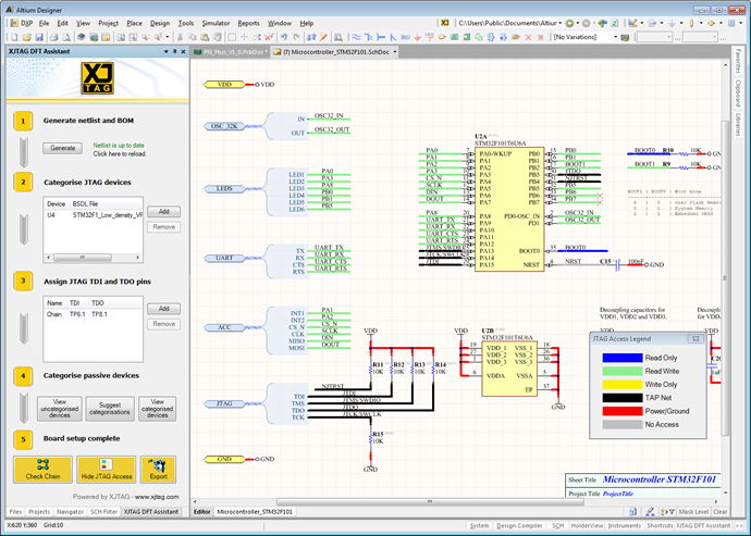
A key feature of the DFT Assistant is its ability to analyse the nets in a schematic diagram and find potential errors in the Boundary Scan Chain(s). As well as verifying the Boundary Scan Chains are correctly routed and terminated, the XJTAG DFT Assistant for Altium Designer is also able to illustrate how much of the circuit is accessible for test using JTAG test equipment. This live visualisation of a board’s Boundary Scan access can be used to improve DFT and ensure in-system programming is achievable, long before the design progresses to layout or is committed to manufacture. Having Boundary Scan available at the prototype stage can also significantly accelerate product development.
Figure 2 (above): The XJTAG DFT Assistant’s JTAG Access view shows clearly how much of the PCB can be accessed and tested using JTAG (nets are colour-coded to illustrate accessibility)

The level of access possible using JTAG is entirely design dependent - if every JTAG-enabled device on the board is correctly connected to a scan chain, and that chain is terminated correctly, access will include all those devices and their associated nets. Using a test system like XJDeveloper from XJTAG, this access can be further exploited to include the functional test of non JTAG-enabled devices, as well as the in-system programming (ISP) of non-volatile or embedded memory and FPGAs/CPLDs. This is the power of JTAG - its ability to provide a high level of access for test and ISP, through a single 4-pin connector. The cost of not implementing the scan chain correctly could be no JTAG access, but with the XJTAG DFT Assistant for Altium Designer, the verification of the scan chain(s) at the schematic capture stage can now be automated, leading to a higher degree of right-first-time, saving design effort and money.
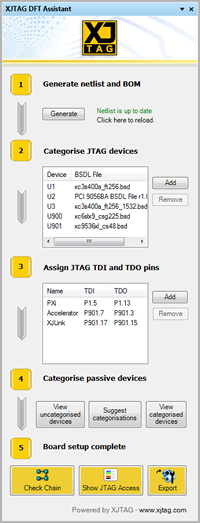
Figure 3 (right): The XJTAG DFT Assistant docks in the Altium Designer environment, providing easy access to its features.
Conclusion
For several decades, tools that provide design automation have been used to increase productivity in engineering disciplines that couple creative input with accurate implementation. While creativity requires free thinking, design is often constraint driven and bringing the two closer together involves an appreciation for what can and can’t be automated.
Through the unified nature and extensibility of Altium Designer, it is now easier to bring design automation to every stage of product development; from design through to manufacture and test.


