Get smart with wireless charging
Wireless charging is the next big wave in portable electronics. And, as Maxim Integrated’s Scott Kim, Nazzareno Rossetti and Raymond Park explain, the elimination of charging cables will change the landscape for powering wearable devices.
Despite its potential, this field of charging is still young, with competing technologies and no definitive standard. Like other critical blocks for portable gadgets, the wireless power receiver must utilise minimal space while meeting the expectation to operate on a single charge for a long time.
Accordingly, the receiver must be very small, highly efficient and compliant with multiple standards. This article discusses the challenges of designing an inductive charging wireless power receiver in today’s climate. It introduces an innovative solution that, in addition to addressing these challenges, enables wireless power transfer to a peer device.
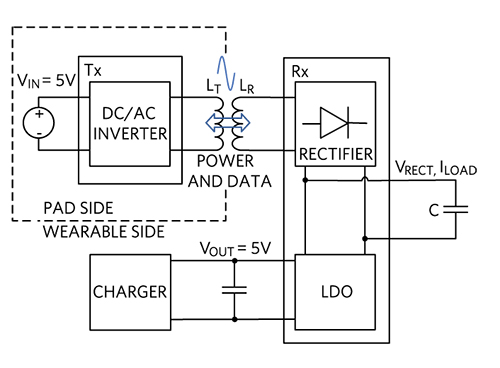
Below: Figure 2. A wireless charging system
Wireless charging system
Figure 2 is a high level illustration of an inductive wireless charging system. The charge is automatically initiated by simply placing the device on the charging pad. The transmitting coil, LT, resides in the charging pad and generates an AC signal of a few hundred kilohertz (WPC and PMA).
The energy transfer happens via the magnetic coupling between the transmitting coil and the receiving coil, LR, in the smartwatch. The AC signal is rectified (VRECT) inside the receiver (Rx) and regulated with an LDO. While power flows forward from the transmitter (Tx) to the receiver, a wireless data signal travels backward, reporting the receiver status to the transmitter. In response to the receiver status the transmitter modulates the transmitted voltage amplitude.
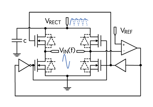
Figure 3. AC/DC active bridge rectifier
Under heavy load, the rectified voltage (VRECT) is kept very close to the output voltage (VOUT) to minimise the LDO losses. Under light load, VRECT is kept high in anticipation of the negative spike that occurs with the application of a heavy load with a fast rising edge. The overall system operates as a low bandwidth closed-loop voltage regulator.
Wireless power transmission standards
Currently, there is no single standard regulating the wireless transmission of power and data from the receiver to the transmitter. Two common standards are PMA and WPC/Qi, both of which are based on inductive charging but with distinctive differences both in power and signal transfer. Both standards require a proximity between the charger and receiver to be between one and a few centimetres. Wireless transmission of power over greater distances is also starting to emerge.
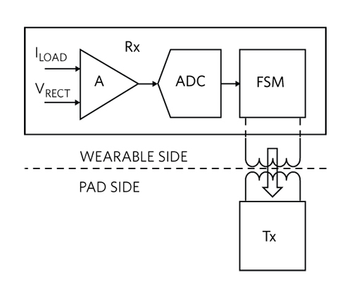
Figure 4. VRECT feedback loop
Wireless charging constraints
Wireless charging eliminates the need to carry a charger or a USB cable while on the go. However, it requires charging pads to be readily accessible. We are now starting to see banks of charging pads available in hotels, restaurants and airports, making this feature increasing accessible.
A state-of-the-art solution
A state-of-the-art wireless charger must address the challenges mentioned earlier, it must conform to multiple standards, have extremely low power consumption, small size, and the ability to work with available charging pads.
The MAX77950 is an advanced wireless power receiver IC that meets the specification requirements for WPC Low Power v1.2 and PMA SR(v2.0) communication protocols. This device operates using near-field magnetic induction when coupled with either a WPC or PMA transmitter and provides up to 12V of output power.
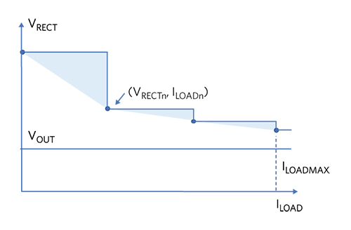
Figure 5. Typical Rectified Voltage Profile
Active bridge rectifier
At the heart of the wireless receiver is a transistor bridge rectifier (Figure 3) that not only takes in the AC input voltage VIN(f) (a sinusoid of amplitude VIN and frequency f), but rectifies it and filters it. The four low RDSON, n-channel transistors within the rectifier greatly reduce the power losses compared to a classic diode bridge rectifier implementation. The dashes outline the MOSFETs intrinsic diodes.
Finite state machine
The VRECT output voltage versus load current must meet the specified profile for the application. To this end, the VRECT and corresponding current, ILOAD, are measured (via amplifier A), digitised (via the ADC) and fed to a Finite State Machine (FSM). The FSM compares the information to a predefined profile table for VRECT vs. ILOAD and calculates the optimum ‘next’ value for VRECT. This information is fed back wirelessly to the transmitter, which adjusts the transmitted amplitude accordingly (Figure 4).
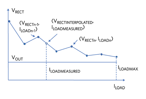
Figure 6. MAX77950 Rectified Voltage Profile
Typical rectifier output profile
The closed-loop system controls the rectified voltage, VRECT, to minimise the power losses across the LDO. For a given application, the voltage profile for VRECT is specified by means of a number (n) of coordinates (VRECTn, ILOADn) in the voltage current space. These coordinates are loaded into chip registers via the I2C bus. Figure 5 is a typical example, allowing for four different levels of the VRECT voltages as a function of the load.
With such coarse granularity, the triangular area under each step, as indicated by the shaded regions, corresponds to wasted power.
MAX77950 rectifier output profile
MAX77950 allows for eight coordinates (corresponding to the blue dots in Figure 6). This provides finer granularity for creating a smoother VRECT profile. Additionally, the FSM measures the load current and forces a VRECT voltage (white dot in Figure 6) that is interpolated between the two specified coordinates (dots ‘n-1’ and ‘n’) adjacent to the measured current value.
As a result, the wasted power due to the quantisation error is greatly reduced.
MAX77950 efficiency advantage
The combination of a low loss, active bridge rectifier and a finely adjusted LDO input voltage (VRECT) results in superior efficiency performance. Figure 7 shows the measured system efficiency from VIN to VOUT (Figure 2) for MAX77950 vs. a competitive solution.
As expected, the reduced losses translate into a superior efficiency at mid- and light loads, with a peak advantage of up to 15% at 300mA.
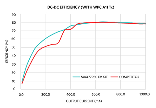
Figure 7. MAX77950 efficiency advantage
Peer-to-peer charging
As an added advantage, MAX77950 implements PeerPower to enable peer-to-peer wireless charging. The IC reconfigures the rectifier block of Figure 3 into a DC-to-AC inverter. The receiving coil now acts as a transmitter to transfer the alternating power to the peer device. Figure 8 illustrates the conversion from DC (VIN(DC)) to square wave (VOUT = ±VIN). Subsequent filtering produces the sinusoidal waveform transmitted to the peer device.
As an example of a typical application, PeerPower allows a wireless transfer of power from a smartphone to a smartwatch. The power drawn from the smartphone is relatively modest but sufficient to recharge the smartwatch. PeerPower is a significant step toward making wireless charging available anytime and anywhere, eliminating the need for the charging pad.
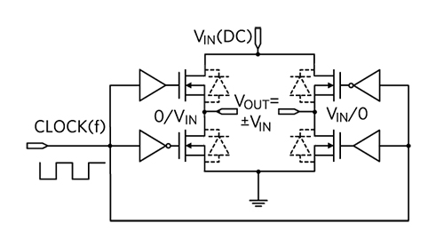
Figure 8. DC/AC active bridge inverter
Small size
For small size requirements, the MAX77950 is available in a small (3mm x 3mm) 12-pin TDFN and in a 12-pin side-wettable TDFN package with exposed pad. The extremely compact packaging combined with the need for very few external components makes the MAX77950 well suited for use in even the smallest wearable designs.
Conclusion
We have reviewed a wireless charging system and outlined the challenges of multiple standards, small size, power efficiency and availability of charging stations. The tiny MAX77950 provides a compact solution. By operating with both WPC and PMA communication protocols, it overcomes the challenge of multiple standards. The superior efficiency allows for longer untethered operation. Peer-to-peer charging moves the industry closer to devices that can be charged anywhere, anytime.


