Digitising linear measurement for greater accuracy
A novel approach to digitally measuring analogue current could deliver greater accuracy at ultra-low powers. By Johann Zipperer & Peter Weber, Texas Instruments.
Measuring current can be as simple as putting a shunt resistor in series with the circuit’s input and measuring the voltage drop using a differential amplifier; the analogue voltage provided by the amp is proportional to the current and can be digitised for further processing.
While this approach works fine in straightforward cases, it fails as soon as things get more complicated. For instance, it is necessary to galvanically isolate the measuring circuits from the live conductor in line-powered applications with high currents and voltages. In this case, instead of using the shunt approach, the solution is to measure the magnetic field surrounding the conductor using hall sensors or magneto-resistive sensors. The shunt principle also fails at the other end of the current spectrum; in applications where current consumption varies widely and may fall to extremely low levels in the nanoamp range. This is primarily the case in ultra-low-power microcontroller circuits used in battery-operated devices. In order to maximise battery lifetime, some kind of energy profiling must be implemented by monitoring the current consumption in many different operating modes.
Such microcontrollers disable any unused on-chip functions in order to save power. In the sleep mode, only a minimised set of functions remains operational and the clock frequency is reduced considerably, resulting in a current consumption in the order of 100nA. However, the current will rise by several orders of magnitude after wake-up. The power consumption of the purely digital functions is relatively low and largely depends on the clock frequency. Power-hungry stages include the on-chip ADCs and DACs, voltage references and operational amplifiers as well as LEDs and radio transmitters on a device level. All in all, the entire system may draw almost 100mA.
For circuit designers, the need to measure currents in such a wide range results in tremendous challenges. It is easy to see that shunts cannot be used here. For extremely low currents, a very high resistance value would be required in order to yield an appreciable voltage drop. On the other hand, this resistance value would make the entire circuit inoperable when the current increases. A switchable shunt would also be impractical. Furthermore, an additional problem would result from the capacitor which buffers sudden load variations at the microcontroller’s power-supply pins. The shunt would result in a small voltage dip when the current rises and the capacitor would be recharged after this. The current waveform in the supply line would then not be identical with the microcontroller‘s current consumption anymore.
Replacing analogue measurement
A new solutions was needed; using magnetic fields for current measurements is common practice in the heavy-current field, but not an option with the small currents used here. And while a current-mirror circuit based on a dual MOSFET was considered, suitable devices are difficult to find and expensive. In addition, this approach only lends itself to high currents and suffers from very low accuracy at low currents. Other techniques also turned out to be impractical. For instance, with a switching regulator operating in PWM mode, the duty cycle could theoretically be used to determine the current. In the real world, however, measurement errors will result from the inevitable manufacturing tolerances of the inductor, among others.

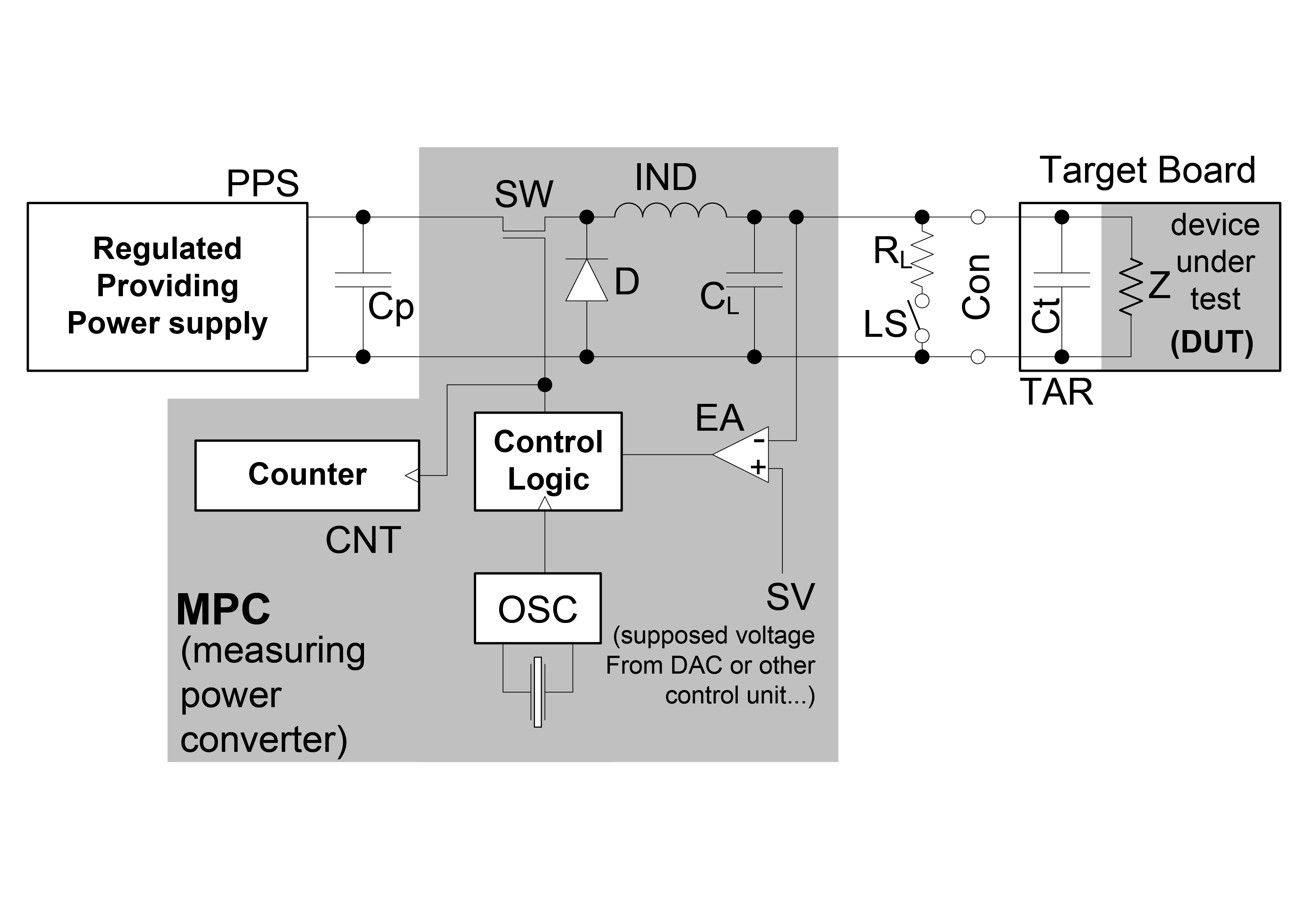
Figure 1 - Block diagram of a switching regulator used for current measurement
A developer team at Texas Instruments in Freising (in the vicinity of Munich/Germany) found an unconventional solution which operates ‘digitally’ to some extent because the operating energy is not supplied to the load continuously, but in small increments which are subsequently counted. A switching regulator (a buck converter in this case) is another core element which in its most basic implementation consists of a switching transistor (SW), an inductor (IND), a diode (D) and a storage capacitor (C1), as shown in Figure 1. The circuit is powered from the stabilised voltage source PPS whose output voltage is buffered by capacitor Cp. The converter’s output powers the external load (i. e. the microcontroller with its widely varying current drain) with an additional capacitor (Ct) connected in parallel. If necessary, a constant load (i. e. a known resistor) can additionally be connected using a switch.
This variant includes a special trick: The switching regulator is not operated the usual way at a constant frequency with a variable duty cycle. Instead, the on-time is fixed, stabilised by the crystal oscillator OSC. The frequency and the component values were selected such that the energy stored in the inductor during SW’s on-time is small compared to the energy stored in the capacitors CP and CL. In order to monitor the output voltage, the error amplifier EA compares the actual value with the desired value (SV). If the voltage is too low, the switching transistor is switched on for the specific fixed interval (one or more periods in the practical implementation) at the next clock edge. At a typical oscillator frequency of 16MHz, the interval will be 62.5ns or a multiple thereof.
The inductor will then extract some energy from CP and transfer it to CL during the transistor’s off interval. This will only have a very small influence on the voltages at CP and CL. Sufficient voltage may be present at CL during the next couple of clock pulses, so the error amplifier will not indicate that the voltage is too low. Due to the continuous current flowing into the load from CL, the voltage at CL will decrease until the error amplifier determines that the voltage is too low after a couple of clock pulses. The transistor will then be switched on again for a fixed time, thereby repeating the whole sequence. Therefore, the off time (and the switching frequency) will vary depending on the load. In each cycle, the same amount of energy will be transferred from the input to the output. If more current is drawn, the number of cycles per second will increase accordingly. In other words, the frequency will be proportional to the load current. In order to achieve a linear relationship, the voltage at CL and CP must be constant. This, in turn, is guaranteed by stabilising the source PPS and the stable reference voltage SV. The number of pulses counted by CNT during a specific interval is a measure of the amount of energy (and of the current, if divided by the measurement time and the output voltage).
Practical experience has shown that this approach is feasible over several orders of magnitude, featuring high linearity for currents above 100nA. Although the accuracy becomes worse below this level, this method is still adequate for estimations. Losses resulting from voltage drops at the diode and parasitic capacitances as well as manufacturing tolerances of the components are equal for all pulses, making the measurement accuracy much better than with the PWM approach mentioned at the beginning. The circuit only requires a single initial calibration using the known reference resistor which is connected to the output instead of the microcontroller.

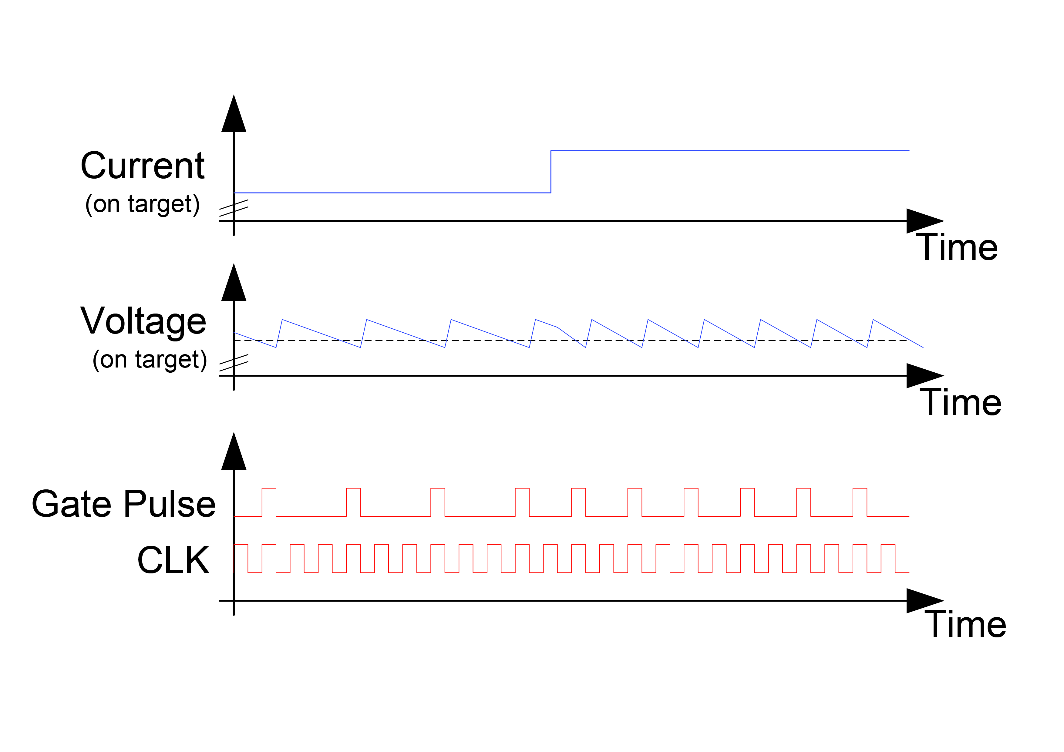
Figure 2 - The circuit’s residual sawtooth-shaped ripple is no issue. The switching frequency rises at a step change from a small current to a high current, resulting in a minor ripple reduction.
As an additional benefit, higher pulse frequencies caused by increased current drain (which may result from analogue sections on the chip) lead to less ripple due to the bypass capacitor.
Practical experience
The number of pulses occurring in a specific interval decreases when the current falls. The measuring interval must therefore be made sufficiently long in order to achieve a specific accuracy. Instead of measuring the pulse frequency, the distances between pulses can be measured, taking less time when frequencies are very low. In this case, the reciprocal value can be computed by the analysing software.
Circuits using different component values were built at TI. Two variants based on a clock frequency of 16MHz are compared below. Both used the pulse-density measurement approach instead of measuring cycle duration.
Variant 1
- Software-Controlled with a MSP430 MCU
- Minimum pulse width: 62.5ns (one period)
- Minimum pulse repetition time: 32 clocks/2µs
- Current measurement range: 100nA to 30mA
- Measuring time for a resolution of 100nA: 1s
- Measuring time for a resolution of 30nA: 10s (due to the system’s noise floor)
- BOM: $4.00
Variant 2
- Software-Controlled with Hardware Support
- Minimum pulse width: 187.5ns (3 oscillator periods)
- Minimum pulse repetition time: 16 clocks/1µs
- Current measurement range: 500nA - 100mA
- Measuring time for a resolution of 500nA: 1s
- BOM: $3.50
Just for comparison: A current measuring device featuring highest sensitivity (e. g. from Agilent) offers a resolution of 100nA at a measuring time of 140ns and costs about $60,000.
Apart from its enormous dynamic range, the described approach offers additional advantages. It is a low-cost method because regular off-the-shelf components are used, it is readily available and it is very small. Its disadvantages, which include less than optimum efficiency, intrinsic energy demand and emissions, are acceptable. The fact that the battery must be charged less frequently is beneficial in practical applications.


