Sensor evolution
How sensor technology is changing in order to meet growing demand from the handheld device sector. Dr Seong-Min Choe, Team Manager of New Market Development, Display Solutions Division, MaganChip Semiconductor, discusses in this ES Design magazine article.
Since the first P-N-P Germanium transistor was invented in 1947, semiconductor laboratories and companies have been providing electronics industry with 70+ kinds of semiconductor devices for rectifying, amplifying, switching, memory, lighting, actuating, sensing, energy harvesting and so on. Diodes and metal-oxide-semiconductor transistors are widely used in mass volume, from power management to computing, in applications ranging from consumer to industrial. Meanwhile, major sensing devices evolved mainly in specific applications such as control systems, medical instruments, and automotive. The semiconductor sensor industry has carved out a specialty niche thanks to multi-principal state-of-the-art of device physics, analogue circuitry design and production technology that lies outside the traditional fabless-foundry business model.
Demand spurred by handheld devices
For consumer products, optical image sensing has been one of the most successful sensor applications since Kodak introduced the 1.3 Mega pixels CCD, KAF-1300 sensor in the late 1980s. Following optical image sensors, different types of sensors penetrated into a series of smart phone segments to play key roles in differentiating UX (user experiences) amongst the growing number of established and emerging manufacturers. They are mainly used for ‘user context recognition’, environment monitoring and creative functionalities.

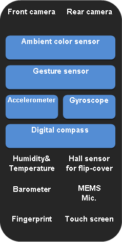
Figure 1: Sensors in a typical smartphone
A recent report from the Gartner Group shows smartphone production growing by a CAGR of 61.6% from 2009 to 2012. According to another recent report issued by Gartner Group, the non-optical sensor market will be growing by a CAGR of 12.1% from 2012 to 2017, which is partially attributed to the increasing number of sensors inside a mobile phone. For models manufactured in 2013, there are typically around 13 sensors in a single smartphone, as depicted in Figure 1. Therefore, a device that most of us carry in one of our pockets today provides a perfect example of how sensors are evolving to meet the demand from the smartphone and tablet sectors.
Fusion and integration
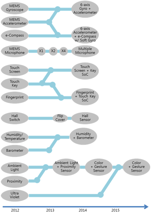
As a primary factor, more and more sensors will be equipped to help OEMs create a better user experience and to win in a growing and fiercely competitive market. But, a fascinating smartphone containing these sensors must not grow in size or consume more power, as compared to current models, and it must feature robust operation in harsh environments. These market dynamics and system requirements a driving the new trends for sensors, as depicted in Figure 2; namely fusion and integration.

Figure 2: Typical sensor trends — fusion and integration
The fusion function mainly aims to improve sensing reliability and to recognise intended user context properly. This is a kind of collective data processing by operating multiple types of related sensors. For instance, a smartphone calculates its roll/pitch/yaw movements by processing data from both the MEMS gyroscope and the MEMS accelerometer. Similarly, the MEMS gyroscope can be partially emulated with both the MEMS accelerometer and the electric-compass. In other cases, a humidity sensor should work together with a temperature sensor to measure the relative humidity of air. Sometimes, an optical proximity sensor works in tandem with a hall switch to confirm the open/close of a magnet-attached flip-cover.
The integration process will provide many benefits to phone manufacturers and sensor suppliers. These OEMs can save both space and BOM (bill of material) by reducing the number of parts. Sensor suppliers can offer a feature-rich and cost-competitive solution by integrating heterogeneous sensors onto a single die or into a single multi-chip-package. For instance, an ambient visible light sensor and an infrared proximity sensor are integrated onto a single silicon die, which is co-packaged with an infrared LED (light-emitting-diode). Furthermore, it is expected that the industry will integrate a UV sensor into this photo sensor package to measure the solar UV index.
Challenging power and price
To extend battery life of a smartphone, sensors are required to minimise the operating power consumption as well as stand-by current. Reduced operating voltage and suppressed leakage current are good ways to achieve these low power goals. In 2013, the ambient light and infrared proximity combo sensor now operates with a 1.8V single power supply, while most predecessor sensors require 2.5 − 3.6V (typical 3.0V) for core and 1.8V for the I2C interface. In early 2014, the electric compass, and MEMS motion sensors are expected to operate with a 1.8V single power supply, following the photo sensor.
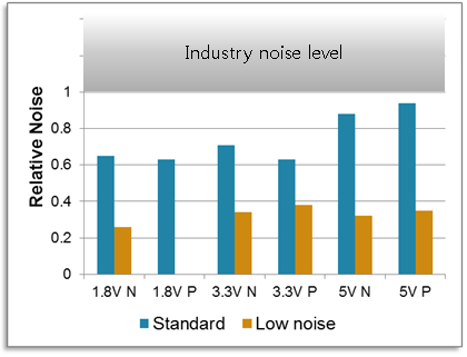
Two silicon technologies are necessary to maintain analogue circuit performance at these reduced operating voltages; a low noise process to suppress the 1/f noise of CMOS transistors operating in the weak inversion region by reduced operating voltage (Figure 3 shows the noise suppression by typical low noise process), and a set of high and low threshold voltage transistors to selectively suppress off-leakage current and to enable multi-stacked topology circuitry.

Figure 3: 1/f noise suppression by typical low noise process
Meanwhile, these sensors are becoming commodity products as market volume soars up, which creates two big challenges; ASP (average selling price) downward price pressure from phone OEMs, and highly flashing demand by the approximately 1 year life cycle of smartphone models.
In response to these challenges, sensor manufacturers are using 8-inch wafers and continue to shrink die size in order to reduce fabrication cost, as well as to maintain mass production capability.
0.18µm advantages
For sensors used in emerging smartphone applications, the 0.18µm node is becoming more competitive than 0.25µm and larger nodes for a number of reasons.
Logic blocks can typically have 35+% area ratio as the fusion and the integration need larger logic blocks to control more sensors and to compute more raw data. A typical 0.18µm 1.8V operating 7-track standard library has 114kgate/mm2 gate density while a typical 0.35µm 3.3V operating 7-track library has only 21.1kgate/mm2.
16bits or 24bits delta-sigma ADC (Analogue-to-Digital Converter) has a huge digital filter block to shrink. Larger sensor elements can be implemented to improve its performance if logic blocks shrink smaller.
1.8V single gate oxide CMOS technology is available for both the 1.8V core and the I2C interface. Further tech node migration requires additional dual gate oxide technology to implement the 1.8V-operating I2C interface.
Low power consumption can be implemented with reduced operating voltage and decreased switching loss. For example, a typical 0.18µm 1.8V-operating 7-track standard library consumes around 0.7nW/gate/MHz while a typical 0.35µm 3.3V-operating 7-track standard library consumes approximately 6nW/gate/MHz.
Sensor products have their own unique technology requirements so we cannot expect all sensors to migrate down to 0.18 micron. For example, a specific MEMS pressure sensor still remains at 6-inch wafer process, whereas many MEMS sensors migrated to around 1.2µm technology node on an 8-inch wafer. However, as the booming handheld device sector demands more and more distinctive applications, some sensors already have migrated down to 0.18µm technology node and more are expected to follow.


