Sensing innovation
Sensors are becoming more prolific as the Internet of Things seeks to connect machines and other inanimate objects with the internet, but the supporting technologies are just as important, as Sally Ward-Foxton finds out in this article from ES Design magazine.
With the advent of the Internet of Things, which is seeking to turn all machines and even some inanimate objects into connected devices, the demand for sensors has never been higher. MEMS accelerometers, in particular, have had a massive impact on consumer electronic devices like mobile phones and games consoles, and the continuing popularity of these devices continues to drive sensor innovation. These applications, which require a large number of relatively small sensor systems, are also increasingly using sensor fusion to generate complex data about the world around them. Sensor technology is evolving at a tremendous rate, but technologies which support these sensor systems, such as sensor platforms and even sensor IC packaging and materials, are just as important as the sensor itself.
Packaging
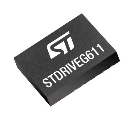
ST has developed a new packaging technology that allows its MEMS sensors to use fully moulded packages. Previously, MEMS sensors were in a cavity-type package with a metallic or plastic cap attached over an organic substrate. A gel was used to isolate the sensors from mechanical shock, which isn’t needed in the new packaging as the sensing element is mechanically decoupled from the package by flexural springs which suspend the sensing element to isolate it from any stress in the packaging. This setup can withstand 10,000g, according to the company, and form factors can be reduced to meet the needs of today’s demanding portable device market.
The advantages of being able to use fully moulded packaging are compelling. The wire bonding is totally enclosed, meaning there is less risk of damaging it during pick and place assembly, while the chances of corrosion are also eliminated. With the old cap-style packaging there was also the risk of damaging or even detaching the cap while mounting the part on the PCB, which just isn’t a factor for fully moulded encapsulation. The soldering process also proved stressful for the sensors — heat and mechanical forces can damage the complex MEMS devices. However, the flexural spring arrangement isolates the sensing element so that it’s free to move, meaning thermal and mechanical stresses are much easier to cope with.
ST has already rolled out this new packaging technology for its accelerometers and gyroscopes, and is transferring that knowledge to its pressure sensor line. The new packaging is set to reduce package size, increase robustness and improve reliability.
Integrating sensors into the wider system can often be one of the hardest parts of development. Freescale’s latest innovation in this area, the Xtrinsic intelligent sensing framework (ISF), allows Xtrinsic sensors or Kinetis microcontrollers to act as a sensor hub. It comprises software infrastructure that provides a run-time environment, alongside unified programming interfaces to make it easy to obtain data from a variety of sensor types.
The framework has power management, bus management, command interpreter and host proxy features (Figure 1). Development of custom sensor algorithms directly on Xtrinsic intelligent sensors is possible and new sensor adapters can easily be added. The idea is to make acquisition of sensor data and implementation of new algorithms as fast and simple as possible.

Figure 1. Freescale’s Xtrinsic intelligent sensing framework (ISF) allows Xtrinsic sensors or Kinetis microcontrollers to act as a sensor hub. The framework has power management, bus management, command interpreter and host proxy features.
Communications
The SENT (Single Edge Nibble Transmission) protocol was introduced to replace inaccurate analogue signalling between sensors and microcontrollers with a simple, low-cost, digital protocol. It’s point to point and unidirectional; messages can only be sent from the sensor to the controller, so no receiver is required on the sensor side, keeping cost down.
SENT-enabled sensors are now available for even the most challenging of environments. Melexis’ range of position sensors includes non-contact 360-degree and 3D SENT solutions for the automotive sector. These multi-dimensional Hall Effect sensors, based on the company’s Triaxis technology, have two pairs of orthogonal sensor elements running in both directions along the surface of a mixed signal CMOS chip. A ferromagnetic film, called IMC (Integrated Magnetic Concentrator) film, is deposited on top of the chip to enhance the magnetic field, thereby increasing sensitivity and lowering noise levels. This has a positive effect on accuracy. As an example, two new additions to the line, the MLX90366 and MLX90367 feature 12-bit resolution and 10-bit accuracy; both are ASIL B SEooC (Safety Elements out of Context) ready. They will find uses in accelerator pedals, electronic power steering, throttle positioning and other automotive and transportation applications.
Materials
The QTC (Quantum Tunnelling Composite) material developed by Peratech has very special properties that make it suitable for sensor applications. Based on conductive filler particles with an elastomeric binder such as silicone rubber, QTC has the ability to change from a near-perfect electrical insulator to a metal-like conductor when placed under pressure. This pressure/force sensing material can carry significant currents and can be directly interfaced to electronic components in a system, making it perfect for sensor development.
Since the material is transparent, it’s an excellent fit for touch screen sensors. One possibility is to add a QTC sensor to a capacitive or resistive sensing application, to add 3D capability; QTC responds proportionally to the force of the touch, which could be useful in gaming applications.
QTC can also be used on its own as a primary touch sensor (Figure 2). It’s so sensitive that a pressure-sensitive QTC sensor can even be placed behind the LCD or OLED screen; no light from the display is absorbed, helping reduce backlighting and save power in mobile devices. An additional advantage is that power is only used when the display is touched, while capacitive solutions need to be powered all the time. EMI is also reduced as a result.

Figure 2. Peratech’s QTC material is force sensitive and transparent, making it ideal for touch screen sensors. It can be placed behind the display so as not to block any light.
Though the material is currently silk-screen printed onto substrates for touch sensor applications, Peratech, in collaboration with the Centre for Process Innovation, is working on new formulations of QTC that will allow it to be printed using industry standard techniques. The plan is to remove one of the final obstacles to entirely printed electronic displays by making the touch sensor printable too, something which is not currently possible. The touch sensor would then be printed alongside the other display components on the production line.
QTC on/off switches will also be printable and further into the future, the company’s E-nose sensors, which detect volatile organic compounds in the air, will be printable too.


