The changing technology of DC/DC converter design and manufacture
Changes in DC/DC converter technology have introduced new materials, digital control and smaller form factors, explains Lars Foerster, DC/DC business development manager, EMEA, TDK-Lambda
DC/DC converters are used in many applications, for example telecomms, data communications, test and measurement, process control, semiconductor fabrication, industrial manufacturing, medical devices and battery powered equipment. They offer a simple way of deriving additional low power outputs from a higher power AC/DC supply, for example a 24V output driving motors, relays or pumps. Alternatively if the system is powered by a 12V battery, DC/DC converters can provide stable, regulated voltages during the battery’s charge and discharge cycles. Controllers, logic circuits and integrated circuits often require single, or dual, 3.3, 5.0, 12 and 15V outputs.
The size reduction of isolated DC/DC converters has been dramatic in the past few decades. In the 1970s, a 1.5W board mount converter measured 45 x 30.5 x 16.5mm (22,646mm3). In 2020, the benchmark for a 3W is 1,642mm3. On average DC/DC converter power density has doubled every 10 years.
DC/DC changes
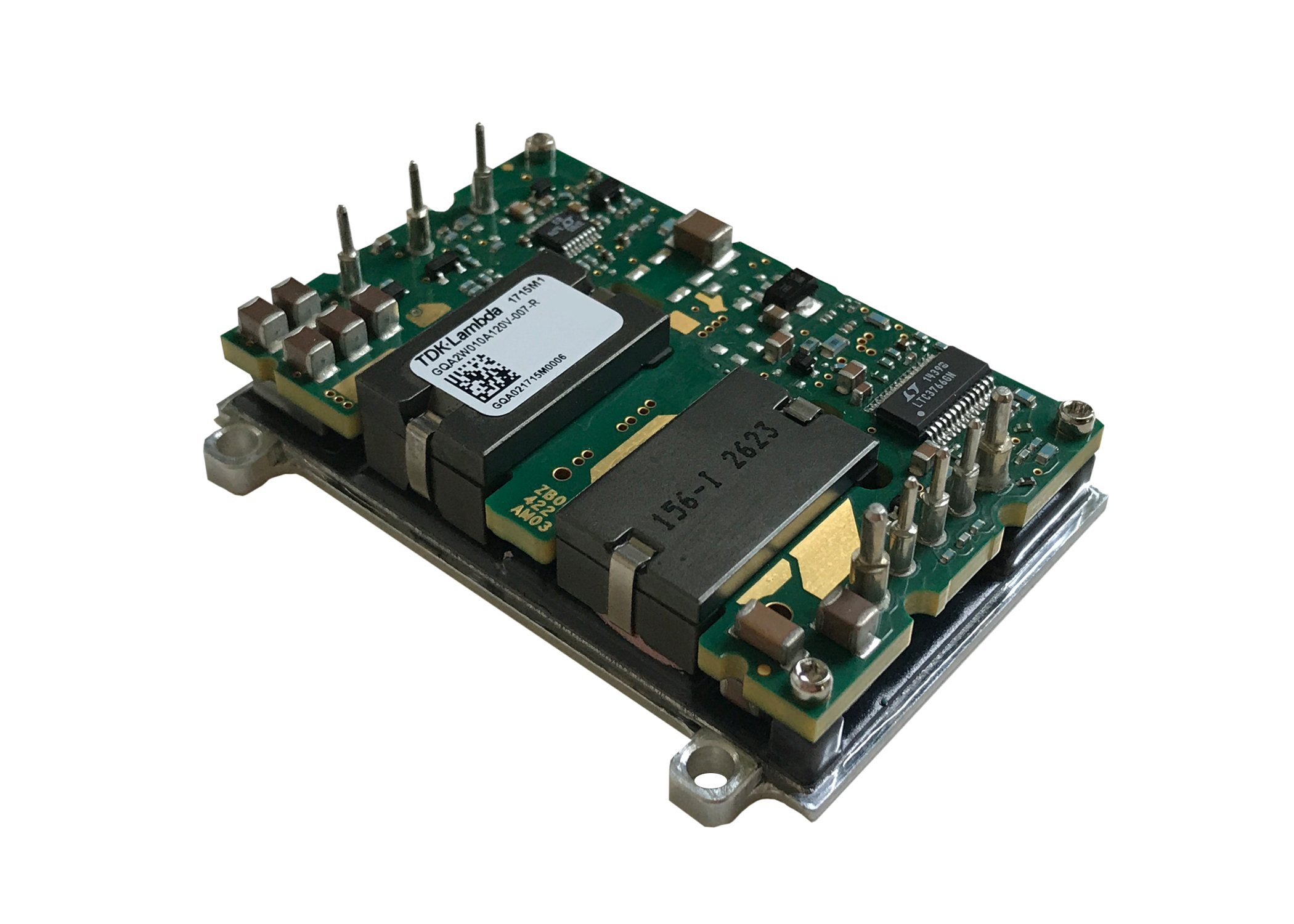
This has been primarily due to major improvements in efficiency as new topologies and techniques have been developed. These include bridgeless rectification, the use of highly efficient GaN (gallium nitride) devices, synchronous rectification and digital control. Low loss ferrite materials have enabled transformers and inductors to dramatically shrink in size. The power transformers on many high power DC/DC models now use integrated copper tracks on a multiple layer PCB as windings. This eliminates traditional wire wound bobbin constructions and the ferrite cores are simply mounted on each side of the board.
 Figure 1: GQA power module with integrated transformer windings.
Higher efficiencies reduce the amount of power dissipated within the supply. Heatsinks can then be made smaller or removed entirely by surface mounting the power semiconductors directly on to the PCB. Multiple-layer glass epoxy construction boards have been superseded by insulated metal substrate (IMS) materials. Copper traces are bonded to an aluminium plate by a high-dielectric insulating adhesive. That aluminium plate can then be mounted to a heatsink or to a cold-plate for convection or water cooling, to dissipate the heat away from the converter.
Higher accuracy surface mount placement allows passive parts to be placed closer together. Smaller component package sizes can be used, with resistors and multi-layer ceramic capacitors (MLCCs) as small at 0603 (0.6 x 0.3mm). Small semiconductors packages are suitable for signal diodes and transistors.
Physical constraints
Some aspects of product design have physical constraints. The international safety agencies mandate how much spacing has to be maintained between the converter’s input and output terminals. Those distances are dependent on the isolation voltage and increase accordingly. As would be expected, the medical IEC 60601-1 safety standard is more severe than IEC 62368-1 for information technology and audio / visual products.
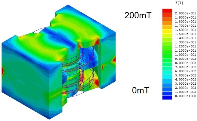
 Figure 2: Magnetic flux modelling for transformer cores.
During product research and development, computer simulation is used extensively. 3D computer aided design (CAD) is used to determine the optimum location of components. Thermal modelling can accurately predict temperature rises. Even the transformer magnetic flux densities can be determined in advance for different ferrite core shapes.
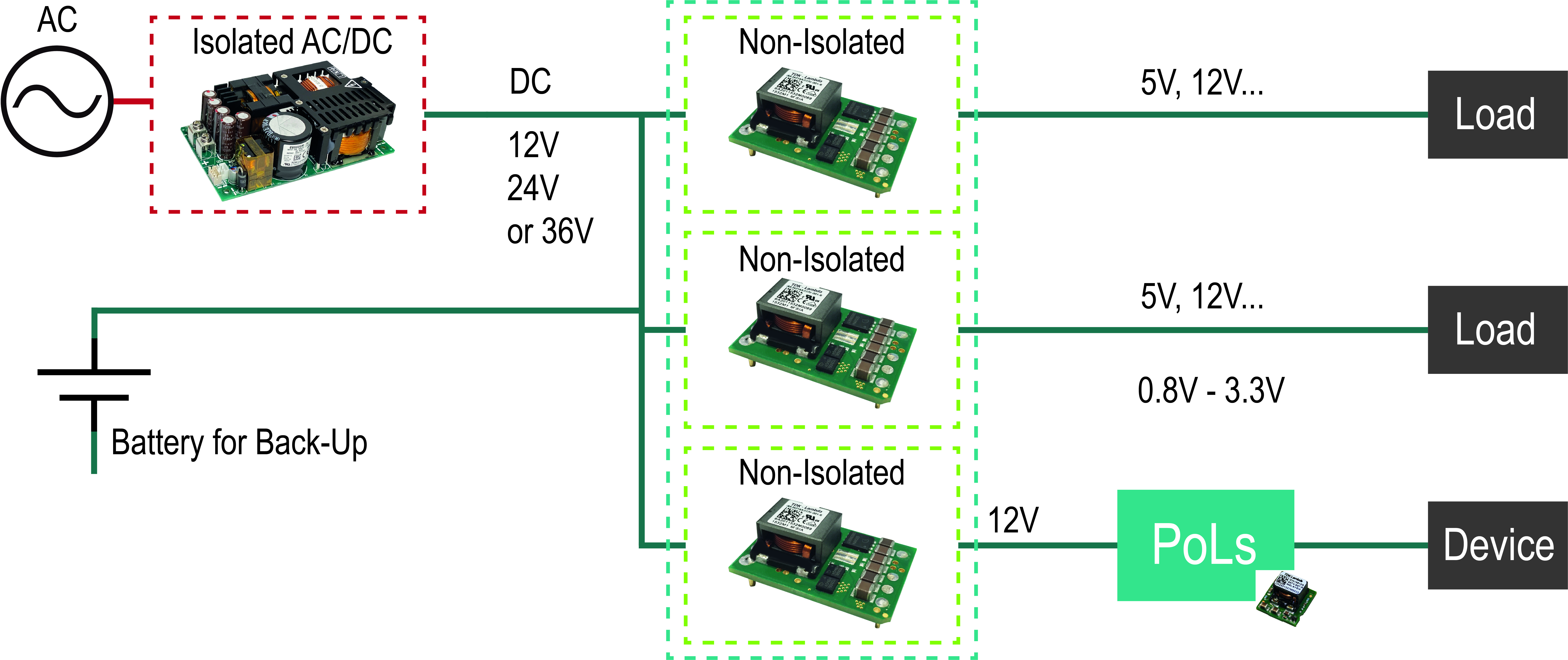
Datacomms and telecomms system cost and technology enhancements have altered the way DC/DC converters are used and what products are needed. This has resulted in new types of distributed power architectures (DPA) being deployed over the last two decades. The supply voltage for ASICs, FPGA and other microprocessors has reduced from 5V to less than 1V. Initially the 24V and 48V DC AC/DC supplies powered isolated DC/DC converters. Now very low cost, non-isolated point of load (PoL) converters, situated next to the processors requiring very fast transient response performance, have replaced many of them. Many datacomms and computing systems now use a 12V AC/DC power supply and the PoLs have wide input ranges, capable of operating from either 5V or 12V DC. Non-isolated DC/DC converters can be used as the protective primary-secondary safety barrier is situated within the AC/DC power supply. This also applies to medical applications.
 Figure 3: Distributed power architecture using non-isolated converters and PoLs.
The power supply control IC manufacturers developed products that board designers can use to create their own non-isolated DC/DC converters. High volume customers created specialised power supply engineering teams, made up of engineers familiar with the technologies. Some power supply manufacturers have announced IC style regulators that can be used to design on-board DC/DC converters. In some circumstances, this seems to be an ideal way of reducing the size of the converter and saving cost. In reality, when the required external inductors and multi-layer ceramic capacitors are included, the board space and cost is greater than a fully integrated, standard off-the-shelf DC/DC converter. The system engineer also has to design the PCB and perform “four corner” testing - at low and high temperatures and at a variety of load conditions. Many engineers are aware that the capacitance can change with temperature, but few know that capacitance can vary considerably with the working voltage.
Changes in design
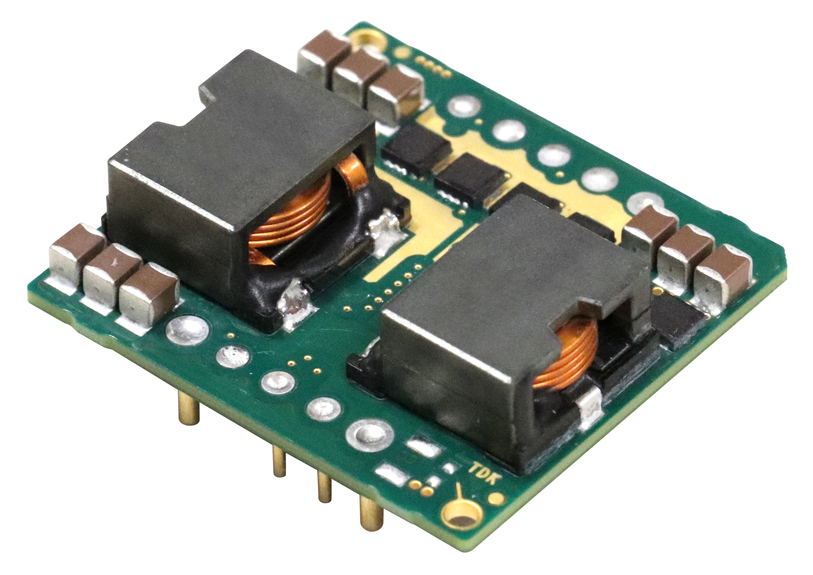
Recently higher power non-isolated DC/DC converters have been launched. These are either buck (step-down), where the output voltage has to be lower than the input voltage, or buck-boost, where the output voltage can be higher or lower than the input voltage. Significant advantages of these converters include a very wide input voltage range, extremely high efficiency (up to 98.5%), low cost due to their simplicity and because of low internal heat losses, very compact sizes. For example, TDK-Lambda’s i7C 1/16th brick footprint buck converter can deliver up to 750W with an input range of 18 to 60V.
Another form of construction has emerged Semiconductor Embedded in Substrate or SESUB. It integrates the power semiconductor and the inductor in a compact module. The IC is contained within the laminate, allowing the inductor (the largest external component) to be placed above it. Through I2C communication the device is fully configurable and suitable for a vast range of applications, including high-performance power management units (PMU) for smartphones as well as Bluetooth modules. A 3.3 x 3.3 x 1.5mm module can deliver up to 6A output current.
Manufacturing lines
DC/DC technology has also been applied through the manufacturing and supply chain, not just with SESUB devices. With 100% surface mount components, robotic assembly allows 24 hours a day continuous production. Just one manufacturing line can provide the capacity to produce nearly 5,000,000 pieces a year. A very high degree of automation has allowed production to be situated in multiple countries, close to the largest customers. This reduces transit times to customer’s factories, reducing product lead-times and the need to hold buffer inventory to save overhead.
 Figure 4: The 16th brick 750W non-isolated DC/DC converter.
Wide range inputs are now commonplace, reducing stock keeping units (SKUs) and inventory. Doubling the input range to 4:1 means that just three models can cover a 4.5 to 76V range. This reduces the number of models to assemble and stock, both for the distributor and the customer. One new model can replace holding a 5V and a 12V nominal input version. Much wider input ranges are possible, but the impact is a reduction in efficiency (and size) and an increase in cost.
Many DC/DC converters have surface mount parts mounted underneath the larger power transformer in a three dimensional structure. This restricts the automated inspection equipment from checking the integrity of the solder joints. Production lines with a high speed X-ray system take pictures from multiple angles and create 3D images. The images of the solder joints are then analysed by computer to determine that the process is correct.
Digital control, high technology levels and new manufacturing techniques are keeping the power supply market abreast, and even ahead, of the demands of the electronics industry.


