Synchronous buck DC/DC IC design
Besides the power efficiency, a key performance requirement for point of load power supply ICs is the transient performance. Sudden changes in the current drawn by the load (for example, an FPGA) require a fast response from the power supply. Such fast variations of the output current, however, cause transient spikes on the output voltage, whose amplitude and duration depend on the transfer function of the regulation loop.
The increasing miniaturisation of semiconductor processes results in lower breakdown voltages of the transistors, and therefore lower supply voltage levels. This in turn reduces the available margin for transient over- and under-voltages on the device’s supply rails. An overshoot above the process’ breakdown voltage can cause the destruction of the device, on the other hand an under-shoot below the device’s minimum operating voltage can cause a malfunction.
Power supply ICs featuring a good load transient performance and a high efficiency ensure sufficient margin to easily design safe power supply circuits while contributing to power savings. Panasonic’s control method used in its latest high current buck DC/DC converters ICs addresses both challenges.
Control modes
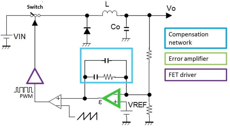
A typical voltage mode controller monitors the output voltage Vo from a single feedback path and compares it with a reference voltage at an error amplifier. A PWM is generated by comparing the error signal with a saw-tooth waveform. The PWM is used as input signal to drive the control FET, as shown in the Figure 1.
 Figure 1 - Voltage mode control block diagram.
A compensation network is required to improve the phase margin of the closed control loop to ensure stability of the power supply. As a result, a larger PCB area is needed for the external compensation circuit. Furthermore, the compensation network and the amplifier slow down the feedback loop’s response.
Stability is often traded for transient response, therefore, the conventional voltage mode control is not the most convenient solution for fast load transient applications.
A current mode controller consists of two loops. An outer voltage control loop tracks Vout. An inner loop tracks the inductor current IL by the sense resistor RS and generates the reference signal used by the PMW generator (see Figure 2).
 Figure 2 - Current mode control block diagram.
The current feedback loops eliminates a complex pole introducedin the closed loop transfer function, and simplifies the loop compensation. This effectively allows the current mode control to be faster than the voltage mode. Moreover, it is easier to use than voltage mode control, as it requires less external circuitry.
However, the current sense resistor affects the efficiency of the system. The current sense loop is also subject to switching noise when the inductor current transits between the low side (represented as a diode in the Figure 2) and the high side power switches. Usually, more complicated methods of current sensing needs to be implemented, increasing the complexity of the controller, which results in a larger silicon area and a higher cost.
Conventional hysteretic control
Conventional hysteretic control is the simplest method, as the feedback loop does not require any compensation. The output voltage is kept within a hysteresis window, defined by a reference voltage. The output of the hysteretic comparator turns the main switch Q1 on/off.
This method’s transient response is the fastest as compared with the voltage mode and current mode, because the transient response time depends only on the delays in the hysteretic comparator and in the driver circuitry.
It does impose a ripple on the output voltage, however, corresponding to the width of the comparator’s hysteresis. The ripple is produced through the ESR (Equivalent Series Resistance) of the output capacitor.
The ripple can be reduced by decreasing the hysteresis width, however there is a design trade-off, as this causes the switching frequency to be higher and the operation to be unstable at some point. At the same time the switching frequency is a function of VIN, VO, L, CO and of the width of the hysteresis window.
Control method
Building on the hysteretic approach, an enhanced controller for a synchronous power conversion circuit overcomes the drawbacks of the conventional method.
The output ripple is suppressed, yet a fast transient response is maintained, noise robustness is ensured, the design is simple with no compensation components necessary, and the method allows user-selectable, stable operating frequency operation.
A ramp wave equivalent to the output ripple voltage of a conventional hysteretic controller operating under the same conditions is superimposed to the reference voltage (see Figure 3). This internally generated ‘virtual ripple’ ensures a sufficient hysteresis width at the comparator while allowing the actual output ripple to be minimised.
 Figure 3 - Panasonic’s hysteretic-based control block diagram.
As the external ripple is reduced and no compensation circuit is required, the number of necessary external components is kept to a minimum and the coil can be under-dimensioned as compared with other control methods.
The output detection voltage Vfb, copied from Vo through a resistive divider, is fed back and compared to the reference voltage Vref to which the ramp wave is added.
When the output detection voltage Vfb equals to the increasing reference voltage Vr while the main switch Q1 is off, the comparison result Vc is reversed and the main switch Q1 is turned on. At this time, a timer used to fix the on time for that period starts counting.
Adaptive on-time control
Following the comparator, an adaptive on-time controller sets the ‘on’ time of the control switch Q1 to a fixed value at each switching period based on the output voltage, the input voltage and the operating frequency set by the user.
Every time the LX switches, noise is injected to the DCDC system. For adaptive on time systems, the noise is critical during LX low to high transition because only the on time is fixed, so the noise injected to the feedback loop can cause multiple LX switching (unstable switching). The ramp control introduces a negative offset naturally synchronised with the low to high transitions of LX, which improves the system noise margin.
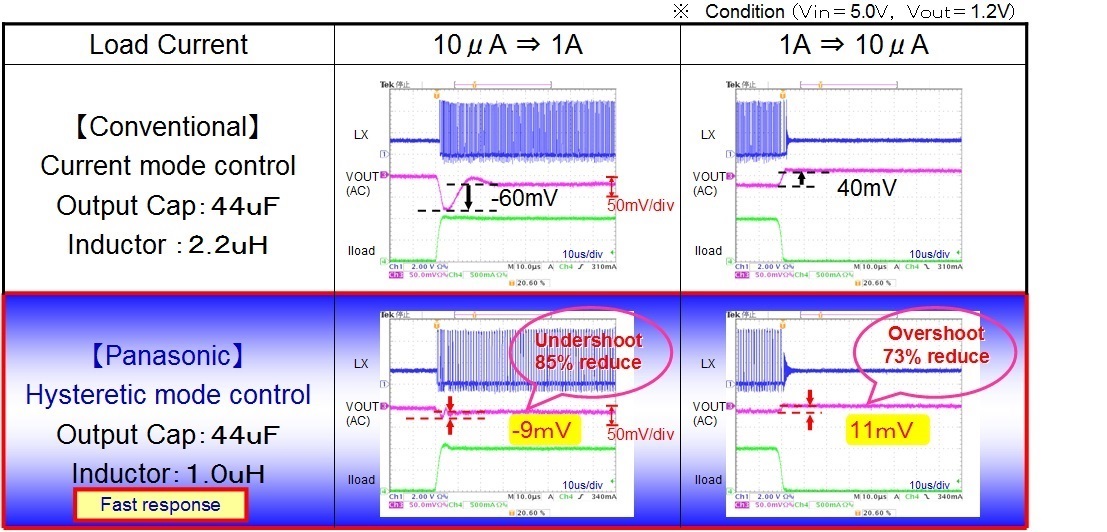
Improvements in response speed and precision achieved by this control method are illustrated in Figure 3. The patented combination of ramp control technology with adaptive ‘on’ time control enables high efficiency, integrated DC/DC ICs with benefits such as increased safety margin under low Vout and high load current and stable operation at fixed controlled switching frequency.
Panasonic MCP DC/DC switching regulators with built in FETs use this control method. Input voltage options range between 4.5 and 30V, output voltages between 0.6 and 5.5V and output currents between 3.0 and 10A in small 4x4mm² and 6x6mm² power QFN packages. The compact size is suitable for PCB power supplies for embedded computing, telecomms equipment, set top boxes, monitors and TVs, storage devices (SSD/HDD), building and security systems.
The switching regulators combine small multi-chip QFN packages, a fast and accurate transient behaviour, high efficiency, due to FET drivers optimised for the built-in, low Ron trench MOSFETs with a selectable frequency operation.


