Quietly powering GSPS ADCs in half the space
Analogue to digital converters (ADCs) have evolved into gigasamples per second (Gample/s) with a corresponding increase in serviceable bandwidth, say Aldrick Limjoco, Patrick Pasaquian, and Jefferson Eco, Analog Devices
These performance improvements come with a number of challenges, one of which is more complex power supply requirements.
The complete ADC power system must be efficient, fit on an already crowded PCB, and produce output noise that matches the sensitivity of the load. Balancing these requirements is an over-riding parametric optimisation problem. Conventionally, the problem is solved by combining switching regulators with low dropout (LDO) post-regulators, which can be relatively inefficient, but they reduce power supply noise. Figure 1 shows the block diagram for a typical system.

Figure 1. Conventional design for a baseline GSPS ADC power supply design using switching regulators and LDO regulators
Efficiency and noise-performance optimisation usually come at the expense of system complexity. Figure 2 shows an alternative power system using µModule Silent Switcher regulators which provide quiet power to the ADC in less space and is more efficient than the conventional solution.
Consider noise
A system designer must consider quantifying the sensitivity of the load and be able to match it to the power supply noise. Power supply noise can be minimised by using a LDO regulator in the power supply path, either as a standalone regulator (Figure 2), or as a post-regulator following a switching regulator as shown in Figure 1. An LDO regulator has the ability to reject input supply noise, measured as its power supply rejection ratio (PSRR).
The trade-off to improve noise performance is lower efficiency; LDO regulators are inefficient at high step-down ratios, as they must dissipate excess power across a pass element. The goal when using LDO regulators is to minimise the step-down ratio to maximise efficiency. This is why they are often used as post-regulators following inherently noisy, but efficient, switching regulators, which initially step-down a main rail before LDO regulator inputs. As a post-regulator, however, maximising the PSRR performance of the LDO regulator requires extra headroom, further degrading overall power supply efficiency, especially at higher loads.
Consider simplicity
Conventional switching-regulator-plus-LDO systems are often implemented using discrete components, resulting in a large, complex PCB footprint. Key regulator components are integrated in the µModule regulators and they can typically handle enough load to allow designers to combine equivalent-voltage power rails on a single µModule output. High current capability also makes it possible to add rails to an existing µModule regulator-based design, simplifying design modifications, and improving time to market.

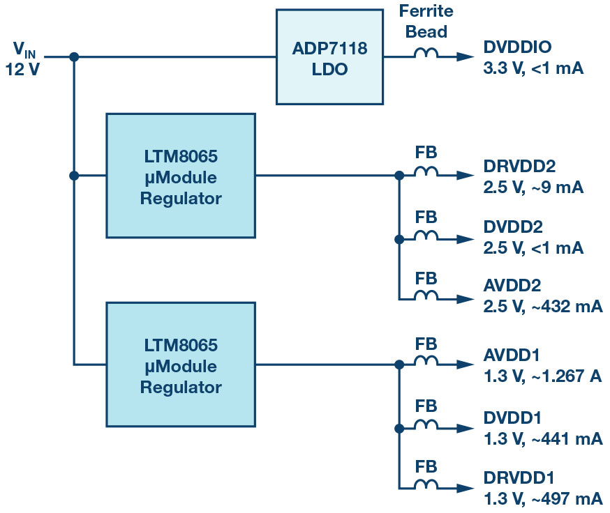
Figure 2: An alternative to the conventional switchers and LDOs power system shown in Figure 1, with two LTM8065 µModule Silent Switcher regulators directly powering an AD9625
To test a µModule regulator solution against a traditional power supply setup, the 1.3 and 2.5V rails of an AD9625 12bit 2.6Gsample/s ADC are powered by an LTM8065 2.5A step-down µModule regulator.
Figure 3 shows two ADP2386, 20V/6A step-down converters with LC filters, the 3.6 and 2.1V intermediate voltages and the 3.6V output regulator. These intermediate voltages are further stepped down by LDO regulators on each regulated ADC input rail. The LDO regulators provide the regulated voltages to the ADC and are effective in diminishing the output ripple from the switching regulators.

Figure 3; Schematic showing the three 2.5 V rails of a traditional switcher and LDO system for powering an AD9625
The traditional, baseline system successfully produced well-regulated, low noise outputs, but at the cost of complexity. It can be difficult to fit the numerous components on the board, and LDO efficiency can suffer at top loads, possibly creating thermal issues.
Figure 4 shows an alternative power solution, with two LTM8065 µModule regulators and a single ADP7118 LDO regulator. The LTM8065 is a 40V input, 2.5A Silent Switcher µModule regulator packaged in a thermally enhanced, compact, over-moulded ball grid array (BGA). The module includes a switching controller, an inductor, and other support components. The LTM8065 supports an output voltage range of 0.97 to 18V and a switching frequency range of 200kHz to 3MHz, with output voltage set by a single external resistor. The only other components required for a complete regulator are the input and output capacitors.

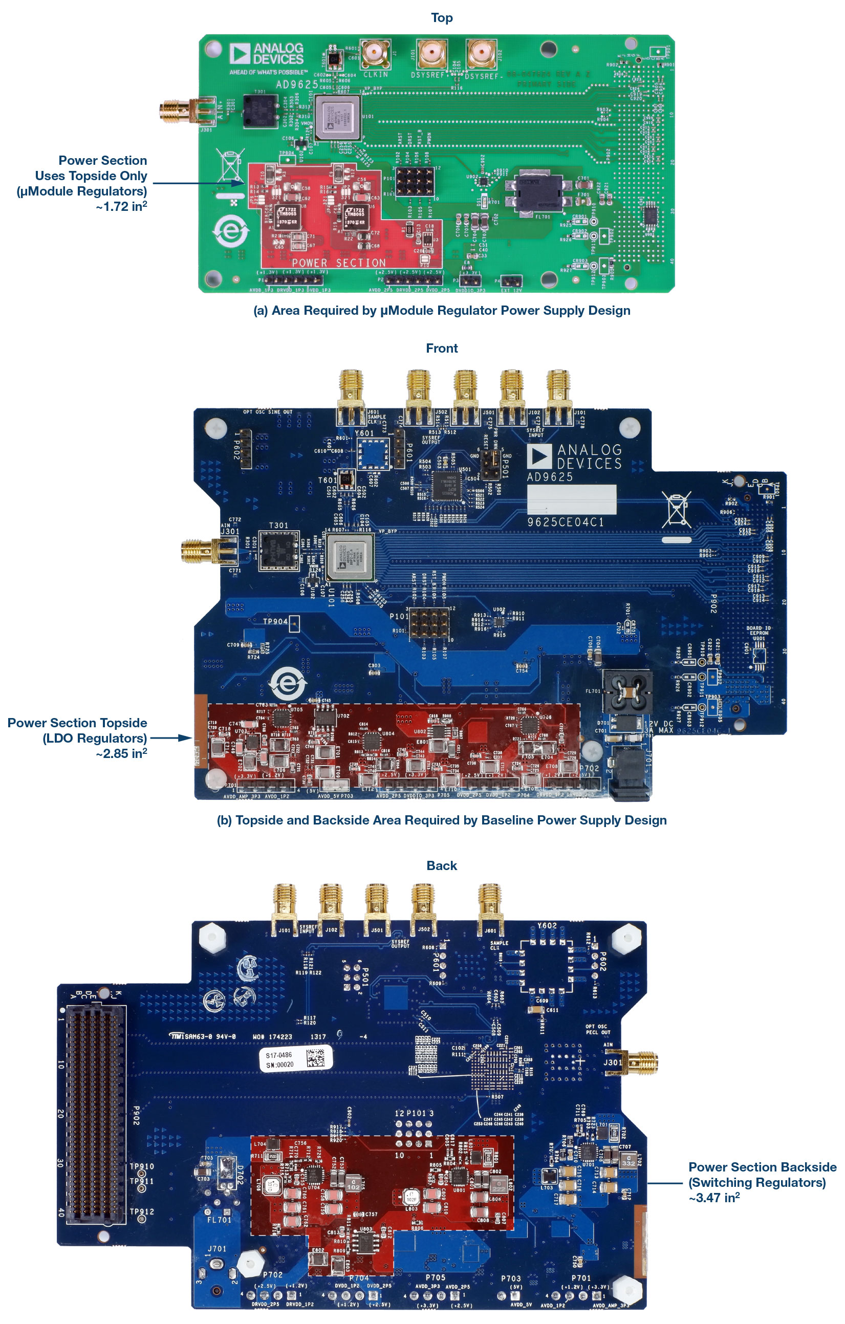
Figure 4: The area needed for a power supply is greatly reduced when using μModule Silent Switcher regulators in place of conventional controllers/regulators
The LTM8065s directly power the 1.3 and 2.5V rails. The 3.3V rail is powered directly by an ADP7118 low noise LDO coming from a 12V supply. The 3.3V rail current is less than 1mA, so power dissipation across the LDO regulator is negligible.
Using an AD9625 2.6Gsample/s ADC, a 1MHz, 100mV peak-to-peak sine wave is actively coupled at the 1.3V analogue supply rail. A corresponding 1MHz digitised spur appears above the FFT noise floor of the ADC, where its amplitude depends on the PSRR at 1MHz. In this case, in the FFT, a 1MHz digitised spur appears above the converter noise floor at −61.8dBFS, corresponding to a peak-to-peak voltage of 892µV p-p in reference with the analogue input full-scale range of 1.1V.
The 1.3V AVDD rail is more susceptible to power supply noise compared to the 2.5V AVDD rail—specifically over the switching frequency range of the LTM8065 (200kHz to 3MHz). Another LTM8065 solution adds a low pass LC (inductor-capacitor) filter for the combined 1.3V rail.
The component recommendation for the low pass LC filter depends on how much filtering is required. For the 1.3V rail, a minimum of 20dB filtering is necessary to reduce the switching spur down to the noise floor of the data converter. A combination of 1.2µH and 4.7µF is used with the cut-off frequency of about 67kHz (~one decade below the switching frequency of the LTM8065 1.3V rail). An inductor with small DC resistance (DCR) is recommended to prevent excessive voltage drop and power dissipation across the inductor.
A multilayer ceramic capacitor (MLCC) has a low effective series resistance (ESR), which provides good attenuation at the capacitor’s self-resonance. The minimum impedance is determined by its ESR. MLCCs also have a low effective series inductance (ESL), which offers excellent decoupling at high frequencies.
Ferrite beads filter high frequency noise produced by the switching regulator at the ADC supply rail. These also provide high frequency noise isolation for each of the combined rails. The recommended current through the bead should be around 30% or less of the ferrite bead DC current rating to prevent the core from saturating, which can lower the bead’s effective impedance and EMI filtering capability. A ferrite bead with low DC resistance minimises the voltage drop and power dissipation across the beads, especially at high current rails such as AVDD 1.3V.
The components of the power solution using the LTM8065 reside almost entirely on the top of the PCB, while the discrete solution on the stock EVAL-AD9625 evaluation board requires power components on both the top (LDO regulators) and the bottom (switcher) sides. The LTM8065-based solution reduces the power supply footprint by over 70%.
Comparing overall component count and component footprint, the LTM8065-based system uses less than half the components in about half the footprint.
Conclusion
The LTM8065 µModule Silent Switcher regulator can power the AD9625 ADC with significant improvements over traditional discrete solutions, without compromising dynamic performance. Significant reductions in component count and power supply board real estate are achieved by using the LTM8065 to directly power the 1.3 and 2.5V power supply rails of the AD9625.
At very high analogue input frequencies, a modulation effect can be observed between the analogue input carrier frequency and the regulator’s output ripple frequency. The appearance of sideband spurs due to this modulation effect are more pronounced at higher analogue input frequencies.
Noise on the 1.3V rail is the main culprit in the modulation effect, due to its low power supply rejection around the switching frequency of the LTM8065 regulator. Although the amplitude of the modulation spurs does not exceed the spurious free dynamic range specification, the spurs can be knocked down with a simple LC low pass filter to attenuate the output ripple.
The µModule regulator power solution achieves a system efficiency of 78%, about a 30% improvement over the existing AD9625 demo board. In addition, PCB board area and component count are significantly reduced.
Visit Analog Devices - Hall 6-442


