Power supply can switch to silent
Addressing PC board layout can reduce footprint, EMI and noise. Tony Armstrong, Analog Devices, explains how Silent Switcher architecture can help power designers
PC board layout determines the success or failure of every power supply design. It sets functional, electromagnetic interference (EMI) and thermal behaviour. A proven way to mitigate the potential threats from EMI from the onset can ensure a quiet and stable power supply. While many switch mode power supply designers are familiar with the design complexities and nuances of switch mode supplies, there are not enough designers in many companies to get all the designs done
More and more, digital designers are being asked to take on switch mode power supply designs. While most digital designers know how to design with a simple linear regulator, not all of their power requirements are step-down (buck mode). In fact, many are step-up mode (boost) or even a buck-boost topology (buck and boost modes combined).
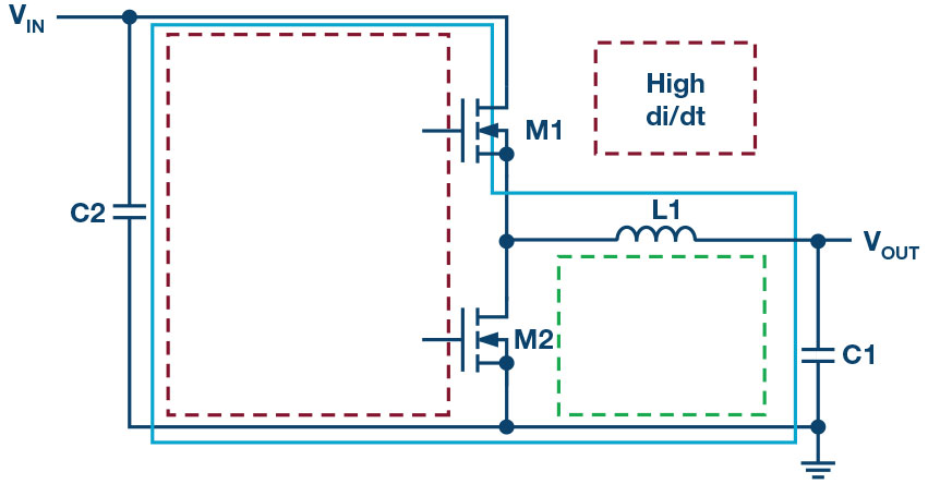
One of the most basic power supply topologies is the buck regulator, as shown in Figure 1. EMI starts off from the high di/dt loops. The supply wire, as well as the load wire should not have high AC current content. Accordingly, the input capacitor, C2 should source all the relevant AC to the output capacitor, C1, where any AC ends.
 Figure 1: Schematic of a synchronous buck regulator
Still referring to Figure 1, during the on cycle with M1 closed and M2 open, the AC follows in the solid blue loop. During the off cycle, with M1 open and M2 closed, the AC follows the green dotted loop. Most people have difficulty grasping that the loop producing the highest EMI is not the solid blue nor the dotted green. Only in the dotted red loop flows a fully switched AC, switched from the zero to I peak and back to zero. The dotted red loop is commonly referred to as a hot loop since it has the highest AC and EMI energy.
High di/dt and parasitic inductance in the switcher hot loop causes electromagnetic noise and switch ringing. To reduce EMI and improve functionality, one needs to reduce the radiating effect of the dotted red loop as much as possible. Reducing the PC board area of the dotted red loop to zero and using a capacitor with zero impedance would solve the problem, however, in the real world, it is the design engineer who must find an optimal compromise.
Managing frequency
Where does this high frequency noise come from? In electronic circuits, the switching transitions coupled though parasitic resistors, inductors, and capacitors create high frequency harmonics. Knowing where the noise is generated, what can be done to reduce the high frequency switching noise? The traditional way to reduce noise is to slow down the MOSFET switching edges. This can be accomplished by slowing the internal switch driver or by adding snubbers externally.
This will reduce the efficiency of the converter due to increased switching loss—especially if the switcher is running at a high switching frequency of, say, 2MHz.
Running at 2MHz enables the use of smaller external components such as capacitors and inductors. For example, every doubling of switching frequency is a halving of inductance value and output capacitance value.
In automotive applications, switching at 2MHz keeps noise out of the AM radio band.
Filters and shielding can also be employed, but this costs more in terms of external components and circuit board area. Spread spectrum frequency modulation (SSFM) could also be implemented—this technique dithers the system clock within a known range. SSFM helps to pass the EMI standards. The EMI energy is distributed over the frequency domain. Although the switching frequency is most often chosen to be outside the AM band (530kHz to 1.8MHz), unmitigated switching harmonics can still violate stringent automotive EMI requirements within the AM band. Adding SSFM significantly reduces EMI within the AM band as well as in other regions.
Alternatively, using Silent Switcher technology can deliver high efficiency, high switching frequency and low EMI.
Switching technology
A Silent Switcher device breaks the trade-off between EMI and efficiency by not needing to slow down the switch edge rates. In Figure 2, the LT8610, as shown on the left. It is a 42V input capable, monolithic (FETs inside) synchronous buck converter that can deliver up to 2.5A of output current. It has a single input pin (VIN) at its top left corner.
 Figure 2: How to make an LT8610 into the Silent Switcher LT8614
When contrasting the LT8610 to the LT8614 (a 42V input capable, monolithic synchronous buck converter that can deliver up to 4A of output current), one can see that the LT8614 has two VIN pins and two ground pins on the opposite side of the package. This is significant, as it is part of what makes the switching silent.
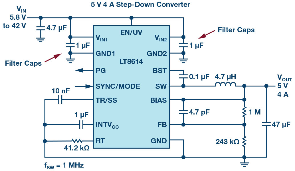
Placing two input capacitors on opposite sides of the chip between the VIN and ground pins will cancel the magnetic fields. This is highlighted in Figure 3, showing the capacitor placement.
 Figure 3: Diagram of the LT8614 showing the filter caps between VIN and ground pins on opposing sides of the IC
The LT8614 incorporates Silent Switcher capability. It can be used to reduce the parasitic inductance by using copper pillar flip-chip packaging. There are opposing VIN, ground, and input caps to enable magnetic field cancellation (right-hand rule applies) to lower EMI emissions.
Reducing the package parasitic inductance is achieved by eliminating the long bond wires of a wire-bonded assembly technique, which induces parasitic resistance and inductance. The opposing magnetic fields from the hot loops cancel each other out and the electric loop sees no net magnetic field.
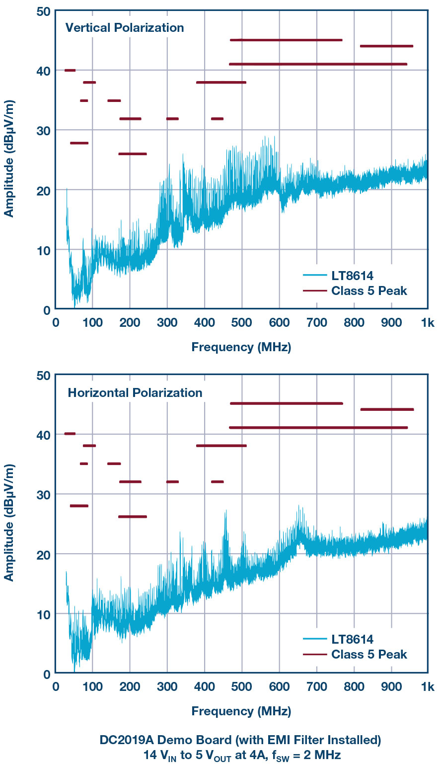
Comparing the LT8614 Silent Switcher regulator against a current state-of-the-art switching regulator, the LT8610 required testing in a GTEM cell using the same load, the same input voltage, and the same inductor on the standard demo boards. There was a 20dB improvement when using the LT8614 compared to the LT8610. This enables simpler and more compact designs where the LT8614 switching power supply needs less filtering and distance compared to other sensitive systems in the overall design. Furthermore, in the time domain, the LT8614 exhibits very benign behaviour on the switch node edges.
Minimising EMI/EMC
The LT8640 step-down regulator features Silent Switcher architecture designed to minimise EMI/EMC emissions while delivering high efficiency at frequencies up to 3MHz. Assembled in a 3.0 x 4.0mm QFN, the monolithic construction with integrated power switches and inclusion of all necessary circuitry yields a minimal PCB footprint. Output voltage ripple is below 10mV p-p at any load, from zero to full current. The regulator allows high VIN to low VOUT conversion at high frequency with a fast minimum top switch on-time of 30ns.
 Figure 4: The LT8614 radiated EMI performance passes CISPR 25 Class 5 limits
To improve EMI/EMC, the LT8640 can operate in spread spectrum mode. This feature varies the clock with a triangular frequency modulation of 20%. When the LT8640 is in SSFM mode, a triangular frequency modulation is used to vary the switching frequency between the value programmed by RT to approximately 20% higher than that value. The modulation frequency is approximately 3kHz. For example, when the LT8640 is programmed to 2MHz, the frequency will vary from 2MHz to 2.4MHz at a 3kHz rate. When spread spectrum operation is selected, Burst Mode operation is disabled, and the part will run in either pulse-skipping mode or forced continuous mode.
Silent Switcher 2 technology integrates the capacitors (VIN caps, IntVCC, and boost caps) inside a new LQFN package, allowing for placement as close as possible to the pins. The benefits included all the hot loops and ground planes inside, all resulting in lower EMI. Fewer external components reduce the footprint and the architecture also eliminates PCB layout sensitivity.
 Figure 5: Schematic shows the differences between LT8640 and LT8640S
Figure 5 shows how the schematics for the LT8640 and LT8640S differ. For example, Silent Switcher 2 technology enables better thermal performance, as the large, multi-ground exposed pads on the LQFN flip-chip package facilitate the pulling of heat out of the package and into the PCB. There is also higher conversion efficiency with the elimination of high resistance bond wires. The EMI performance of the LT8640S easily passes the radiated EMI performance CISPR 25 Class 5 peak limits with a wide margin.
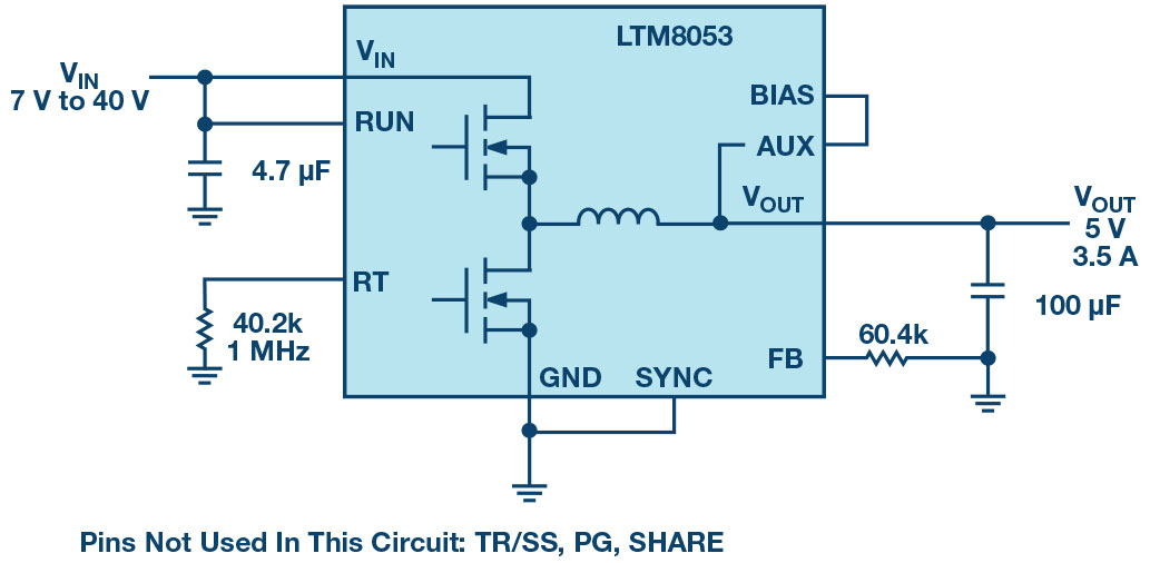
The next step is to incorporate Silent Switcher 2 into the company’s μModule regulator product line. In this form factor, everything is integrated inside a single package and provides simplicity and high power density. The LTM8053 and LTM8073 are micro-module regulators where everything is virtually integrated with just a few capacitors and resistors external to them (Figure 6).
 Figure 6: The LTM8053 Silent Switcher 2 μModule
Silent Switcher capabilities and benefits are designed to make it easier for switch mode power supply designs to pass the various noise immunity standards, such as CISPR 32 and CISPR 25, via characteristics such as high efficiency conversion at greater than 2MHz switching frequency with minimum impact on conversion efficiency, internal bypass capacitors to reduce EMI radiation and reduce footprint and essentially eliminates PCB layout sensitivity. Optional spread spectrum modulation also helps mitigate noise sensitivity. Finally, Analog Devices reports that using Silent Switcher devices saves PCB area and can also reduce the number of layers needed.


