Microcontroller balancing act demands a new process
A new semiconductor process combines lower leakage with low standby current modes, writes Graeme Clark, Renesas Electronics Europe
In today’s increasingly connected world, we are always faced with a large number of conflicting requirements which we have to balance in designs.
Today’s consumers demand ever more complex products, with higher performance and more advanced features. These demands need to be balanced against a reduction of the energy consumed by the application, and of course all at the lowest possible system cost.
Using the standard CMOS process technologies available today, microcontroller designers must also make some tough decisions. They need to balance performance and integration against power consumption, especially with regard to the standby current of the device.
Process nodes
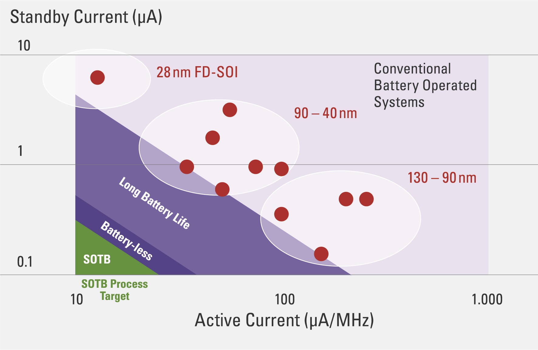
Choosing an advanced process node, typically 40nm (although today’s structure widths are even smaller), enables developers to offer products with high levels of peripheral integration, including large on-chip flash memories of 2Mbytes or more, along with high performance. Operation in excess of 200MHz is not uncommon for such a process. While the active switching current of such a process is typically very low at around 50 to 100µA/MHz, the leakage current from each gate in such small structure widths is very high. This results in extremely high standby currents, typically 10 to 100µA or more.
 Figure 1: Map of process technologies against active and leakage currents
If the goal is to develop devices that combine lower leakage with low current standby modes, it is conventional to choose larger process geometries. This restricts these modules in both performance and the level of integration of memory and other peripherals.
The typical range of values achieved by a range of process technologies available today is shown in Figure 1.
Under the aegis of the Japanese government’s LEAP (Low power Electronics Association and Project) initiative, Renesas has developed a new semiconductor process, Silicon on Thin Buried Oxide (SOTB). The features of this new silicon process avoid the established interdependency between process geometry and power consumption and to develop devices that combine the best low active current with the lowest leakage currents. Using the SOTB process, devices can offer high performance, as well as high levels of memory and peripheral integration. Figure 2 illustrates a comparison between SOTB and the various process geometries.
Hybrid silicon
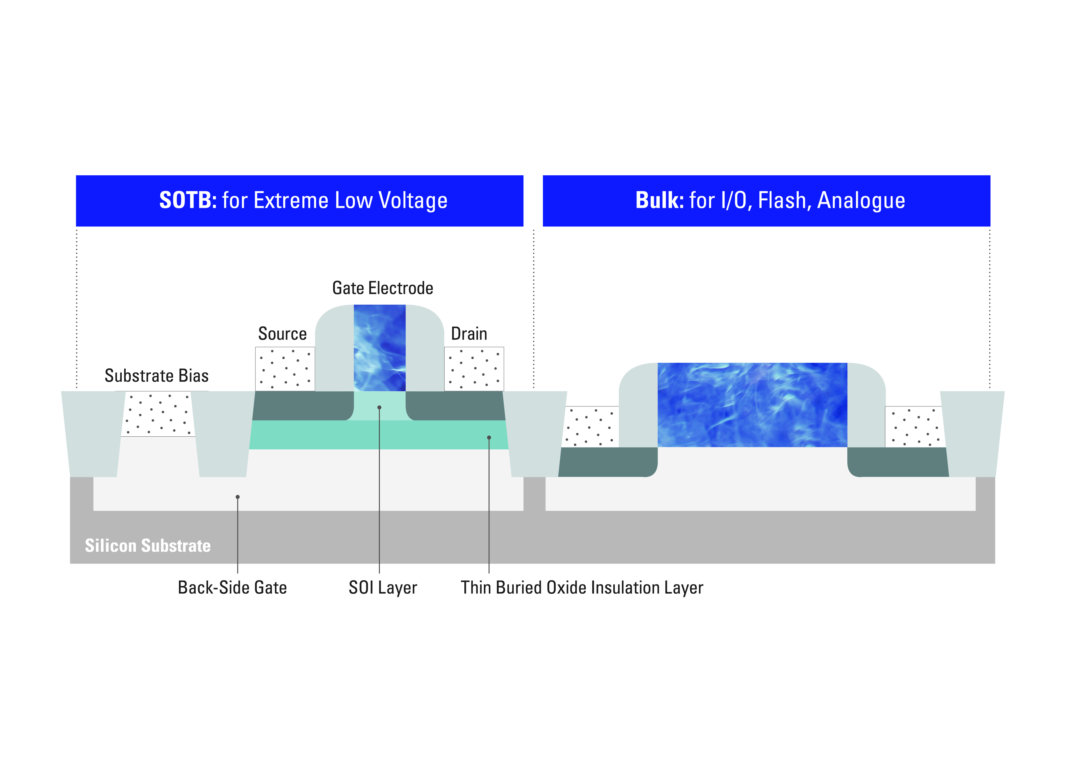
One of the huge breakthroughs in the development of this technology has been the ability to realise a hybrid silicon structure. As this combines the benefits of the new SOTB process and the existing standard bulk silicon technology on the same design, the strengths of both technologies can be used in the same device.
 Figure 2: Comparison of SOTB characteristics with other process geometries
This means SOTB technology can be used in parts of the chip design where ultra-low power consumption is required, but standard silicon can be used for features such as the I/O ring and analogue components. As a result, designers can still work with the devices that have similar electrical characteristics to existing microcontrollers.
Figure 3 shows some of the benefits of the SOTB gate structure. In a traditional bulk silicon gate design, channel impurities or dopant atoms must be injected into the silicon during the manufacturing process, which enables the gate to conduct when required. The number of atoms injected into each gate is extremely hard to control accurately, so the gate characteristics are variable. This is especially the case with smaller silicon geometries as the number of atoms involved is extremely small, sometimes in the region of 100 individual atoms. This means that there can be a significant variability in the number of dopant atoms in each gate, resulting in a significant variability in the switching characteristics of each gate within the device.
 Figure 3: The hybrid structure of the SOTB architecture
The SOTB gate is a dopantless channel design in which the characteristics of the gate are controlled by the extremely thin isolation layer within the gate. Using modern process technology, this is extremely well controlled and is therefore extremely repeatable across the device. As a result, the variation between each gate is much lower than with the traditional bulk silicon gate design. This reduction in the variation between gates on a SOTB device allows the operating voltage to be reduced and hence the energy used to switch the gate is lower.
Figure 3 illustrates another benefit of the SOTB technology, the ability to apply a negative back bias voltage to each gate. This allows manipulation of the switching thresholds of each gate on the device, either individually or across the total device.
Switching performance
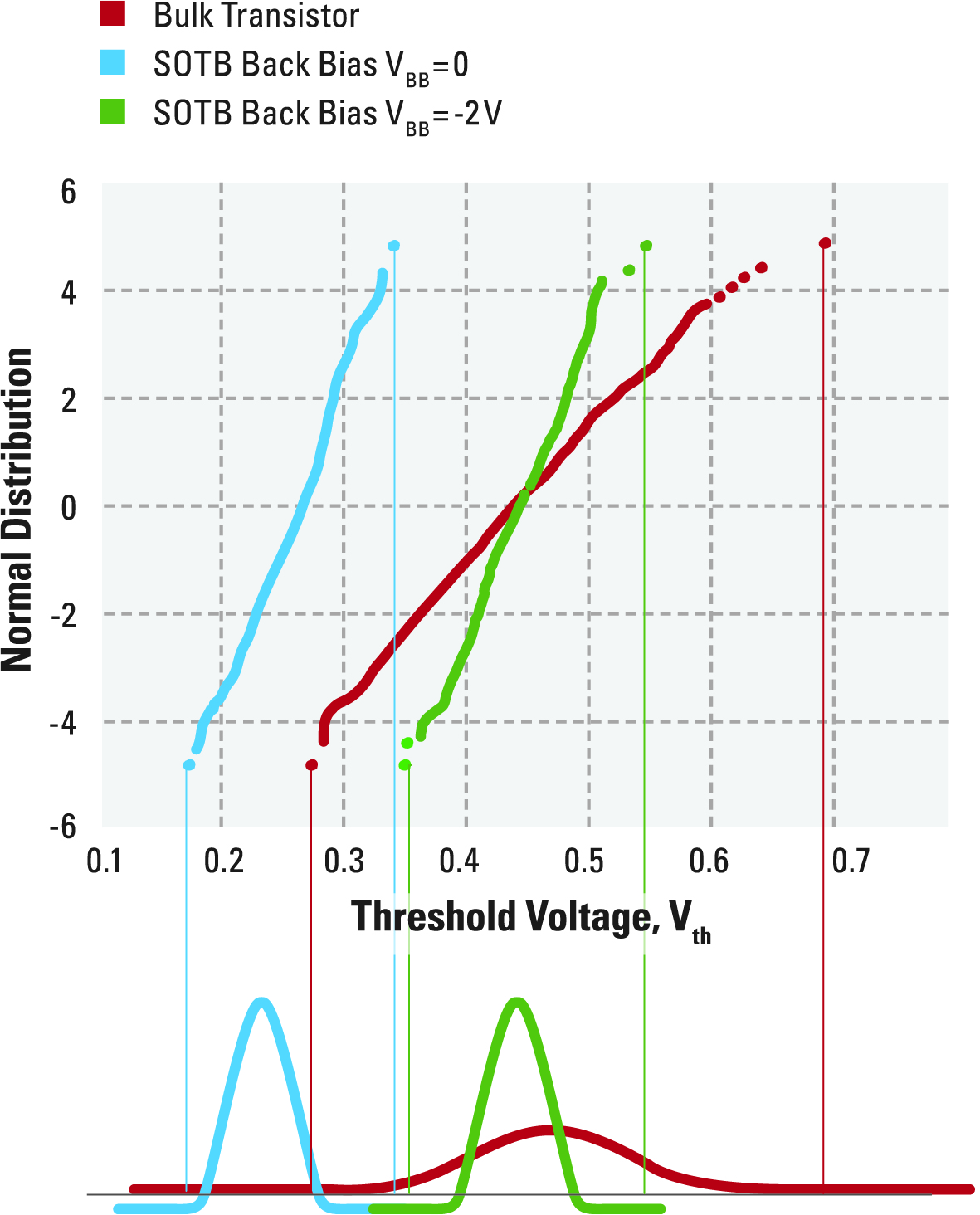
Figure 4 shows a comparison between an SOTB device and a device made on a standard bulk silicon process. The red line shows the range of switching characteristics for a typical device implemented on a bulk silicon process. The variation in switching threshold is between the one million individual transistors on the test chip. The diagram shows that the best gates will switch at around 0.3V, while due to the inherent variability of the process, the worst gates will switch somewhere in the region of 0.7V. In order to guarantee the operation of every gate on the device, it must operate significantly above 1.0V. This has a direct impact on the power consumed by the device.
 Figure 4: Comparison of SOTB and standard process threshold
The blue line in Figure 4 shows the characteristics of the SOTB gate with a huge reduction in variability and the narrow range of switching characteristics that can be achieved with this process. Devices based on the SOTB process can safely run at much lower voltages and guarantee that every gate will operate correctly, resulting in a huge reduction in the value of the active power consumption.
The green line in figure 4 shows the result of the back bias being applied. Leakage can be controlled on individual gates’ in other words, placing part or all of the device into an extremely low leakage state greatly reduces standby current.
The result of this new process is that it enables a paradigm shift in low power microcontroller designs to develop a new generation of microcontroller products. These will combine the best qualities of both smaller geometry technologies with their high levels of integration and low active current and larger geometry, low leakage current devices.
Product development
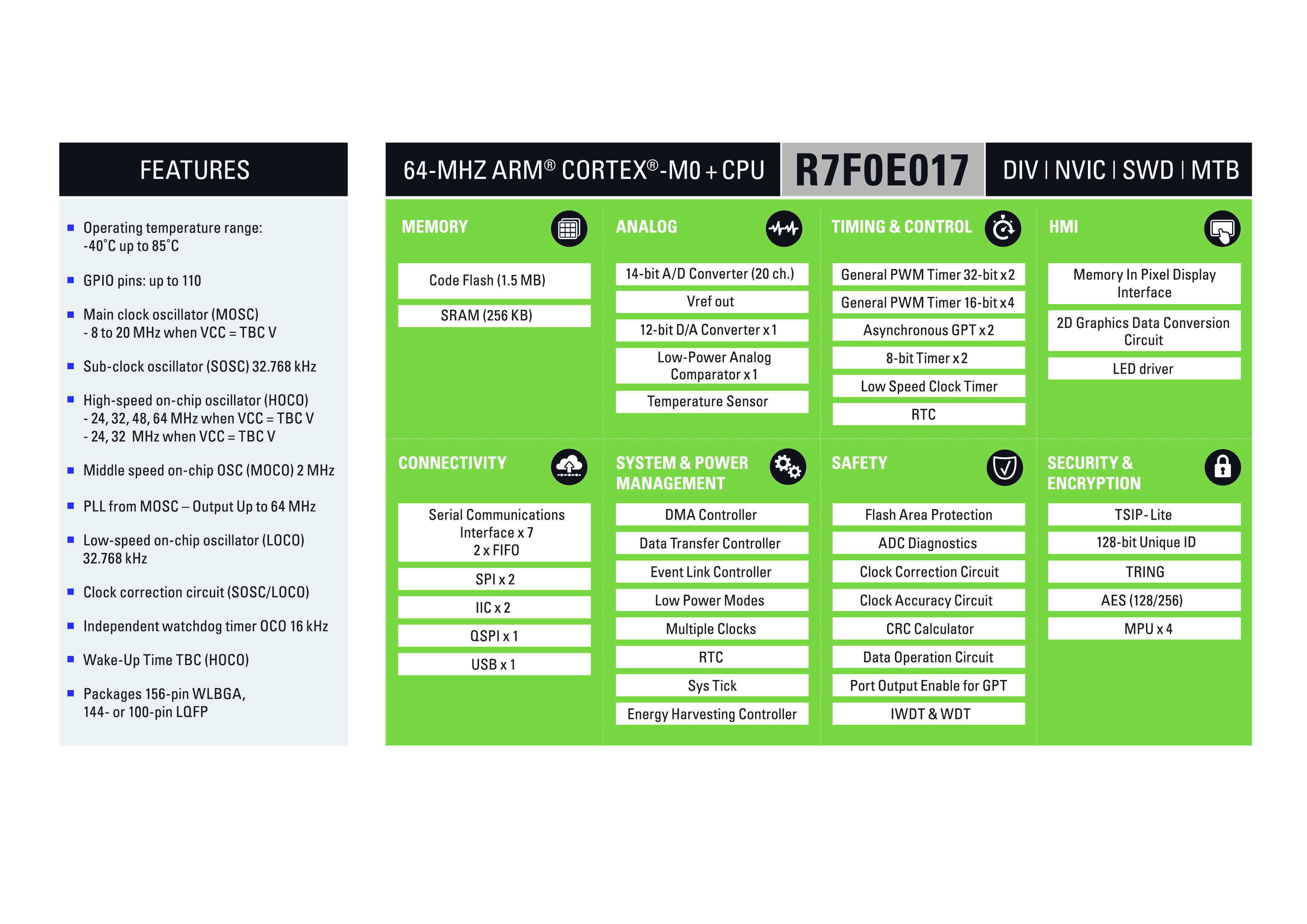
Renesas has now finished development of the first microcontroller using the SOTB process. The use of the SOTB process allows production of a device that is distinguished in the industry with its combination of performance, integration and power consumption. The first device combines a Cortex M0+ core running at up to 64MHz with a high level of peripheral integration and up to 1.5Mbytes of flash and 256kbytes of on-chip SRAM.
The use of SOTB technology on this device has resulted in some dramatic low power characteristics. The first device has active current of 20µA /MHz, standby current of 200nA, ADC operation at 3µA and 256kbyte SRAM with 1.0nA/kbyte standby current. Future devices using this process could offer even lower power consumption.
 Figure 5: The R7F0E017 is the first microcontroller developed using the SOTB process
The first device to use the SOTB process is the R7F0E017. See Figure 5 for an overview of its features. It combines large on-chip flash memory and on-chip SRAM with low power consumption levels, making it suitable for a wide range of applications, including wearable devices, consumer, industrial and medical applications.
The use of SOTB technology also enables the use of these devices in applications that harvest energy from the environment. With this in mind, the R7F017 also includes an energy harvesting controller. As well as allowing energy to be harvested from a range of different renewable energy sources, the controller also enables the device to automatically control an external rechargeable battery or super capacitor.
The development of the SOTB technology will enable the development of a new class of low power microcontrollers suitable for the next generation of connected applications. In addition, it will also enable a new range of energy harvesting applications for many of today’s low power applications.
Samples of the R7F017, along with a complete suite of development tools, will be available to beta customers in early 2019 with general samples available in the second half of 2019.


