Laser technologies drive semiconductor manufacturing
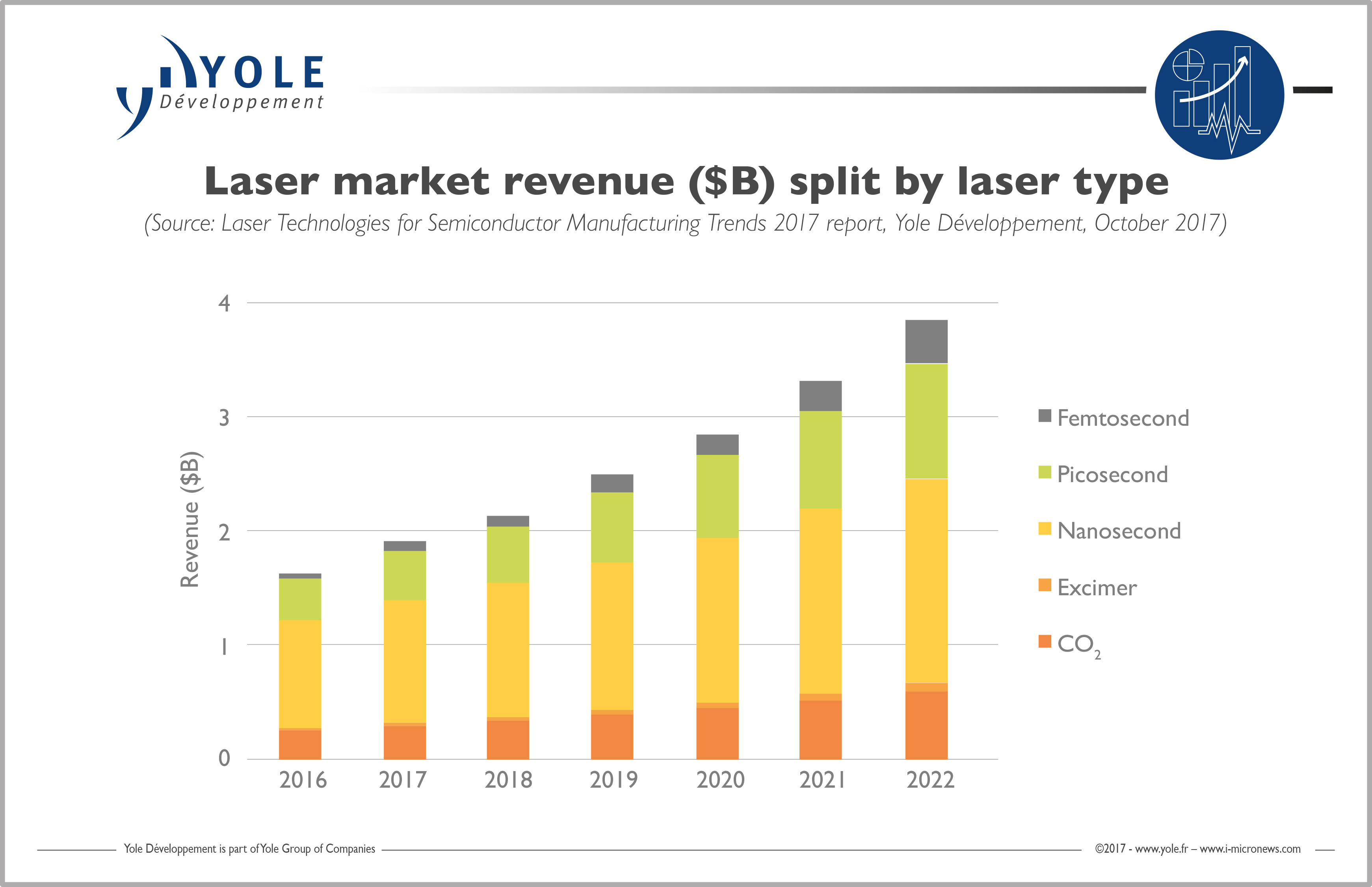
Today a wide variety of laser technologies is available to semiconductor manufacturers and enables the development of innovative semiconductor manufacturing processes. According to Yole Développement (Yole), the laser equipment market will grow at a 15% CAGR between 2016 and 2022 and should reach more than $4bn by 2022 (excluding marking). Those figures are showing the massive adoption of laser technologies for semiconductor manufacturing processes.
In its latest report titled Laser Technologies for Semiconductor Manufacturing, the market research and strategy consulting company details the status of this industry, mainly driven by dicing, via drilling and patterning in PCB flex and PCB HDI, IC substrates and semiconductor device processing.
The Laser Technologies for Semiconductor Manufacturing report from Yole provides a thorough analysis of the different existing laser equipment and laser source solutions developed for semiconductor process steps. It is a comprehensive analysis highlighting the maturity level of each laser type, based on a technical roadmap until 2022. With this new report, Yole’s analysts offer a clear understanding of the laser technologies’ benefits and added value for each manufacturing process.
The Laser Technologies for Semiconductor Manufacturing report is the first of a wide collection of reports that will be released by Yole during the next months. What are the key semiconductor manufacturing processes that are driving the laser equipment industry? Yole invites you to discover today the latest technology challenges and market evolution.
Today, laser applications in the semiconductor industry are broad and diversified. Various laser technologies have started integrating into major semiconductor processes, including laser cutting, drilling, welding/bonding, debonding, marking, patterning, marking, measurement, deposition, driven by motherboards. They are used to process semiconductor devices, flexible and HDI PCBs, and in IC packaging applications.
Drivers of laser methods differ from one process step to another. However, there are similar and common drivers for applicability of lasers to semiconductor and PCB processing applications. The key trends driving laser applicability and contributing to its growth are:
- The desire for die size reduction and thus further miniaturisation of devices driven by computers, hand-held electronic devices such as mobile phones, tablets and electronic book readers, wearable devices and consumer electronics
- Demand for increased yield and throughput
- Better die quality
- The need to inspect voids and particles through a transparent material such as glass, which requires the use of laser methods
- Laser annealing for very high flexibility
However, the choice of the most suitable laser processing type depends strongly on the material to be processed, processing parameters, and the manufacturing process step.
Laser type is defined by parameters such as wavelength, emitting UV, green, or IR light, for example, as well as the duration of pulse, for example nanosecond, picosecond or femtosecond. Users must consider which pulse length and wavelength is right for their semiconductor process step and application.
Nanosecond lasers are the most commonly used type of laser applied in semiconductor manufacturing and PCB processing, with more than 60% market share. They are followed by picosecond, CO2 and femtosecond lasers. In the case of dicing step, the choice of laser type also depends on the material and substrate to be diced. For low dielectric constant (low-k) materials, nanosecond and picosecond UV lasers are used to optimise optical absorption. Picosecond and femtosecond IR lasers are typically used for cutting glass and sapphire substrates but not singulating SiC substrates.
In drilling, the type of laser employed depends on the substrate. Nanosecond UV lasers are usually employed in flexible PCBs, while CO2 lasers are largely applied for PCB HDI and IC substrates. However, for IC substrates, the choice between CO2 and nanosecond or picosecond UV lasers depends on via diameters. Below 20μm diameters, the industry tends to go to picosecond UV lasers which are much more expensive than nanosecond UV lasers but offer superior quality.
Generally speaking, CO2 is the cheapest and fastest laser solution and used in preference to nanosecond, picosecond or femtosecond solid state lasers for dicing, drilling, patterning, marking for applications that require high power and do not care about heat damage or dicing width. However, CO2 is limited when small features are needed. Nanosecond lasers are currently the dominant technology, but picosecond and femtosecond lasers could move ahead in the laser dicing equipment market. However, femtosecond laser implementation is more complex and expensive.
Yole’s laser report will provide a comprehensive overview of the laser equipment and laser sources used for each semiconductor process step application, along with a detailed analysis of laser technology trends and a market forecast. It will also offer a detailed analysis of the laser equipment market by volume and value, its growth for the 2016-2022 timeframe, and breakdown by laser type and process step application.


