GaN for high density servers
The performance of GaN devices in 48V applications extends their use to high performance servers.
Gallium nitride (GaN) devices offer performance in a small form factor, increasing the efficiency, and reducing the system cost for 48V power conversion applications. They have been adopted in high volumes in high density computing, as well as many new automotive power system designs. In all the topologies with 48V input, the highest efficiency, smallest size, and lowest cost comes from using GaN devices.

Figure 1: Key figure of merit, Area x RDS(on) (a)and (b) figure of merit, RDS(on) x Qg
Figure 1(a) shows a comparison of GaN devices to silicon MOSFETs, showing that GaN transistors improve the key figure of merit, Area x RDS(on), by five times at 100V. That improvement results in smaller size and lower cost or lower RDS(on) in the same size. Figure 1(b) shows a second important figure of merit, RDS(on) x Qg, indicating that GaN is also five times better at 100V than silicon in switching speed, resulting in lower losses. Finally, the zero reverse recovery (QRR) and less switching losses of GaN allows an increase in frequency resulting in higher power density. The blue diagonal lines represent the physical limits of silicon MOSFETs.

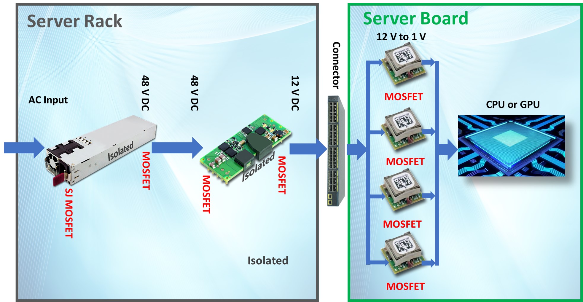
Figure 2: Traditional server architecture
Server bus distribution
Traditional server architecture uses rack-based 48V isolated and regulated DC/DC converters that convert to 12V, then a 12V to point of load convert to the CPU or GPU (Figure 3).

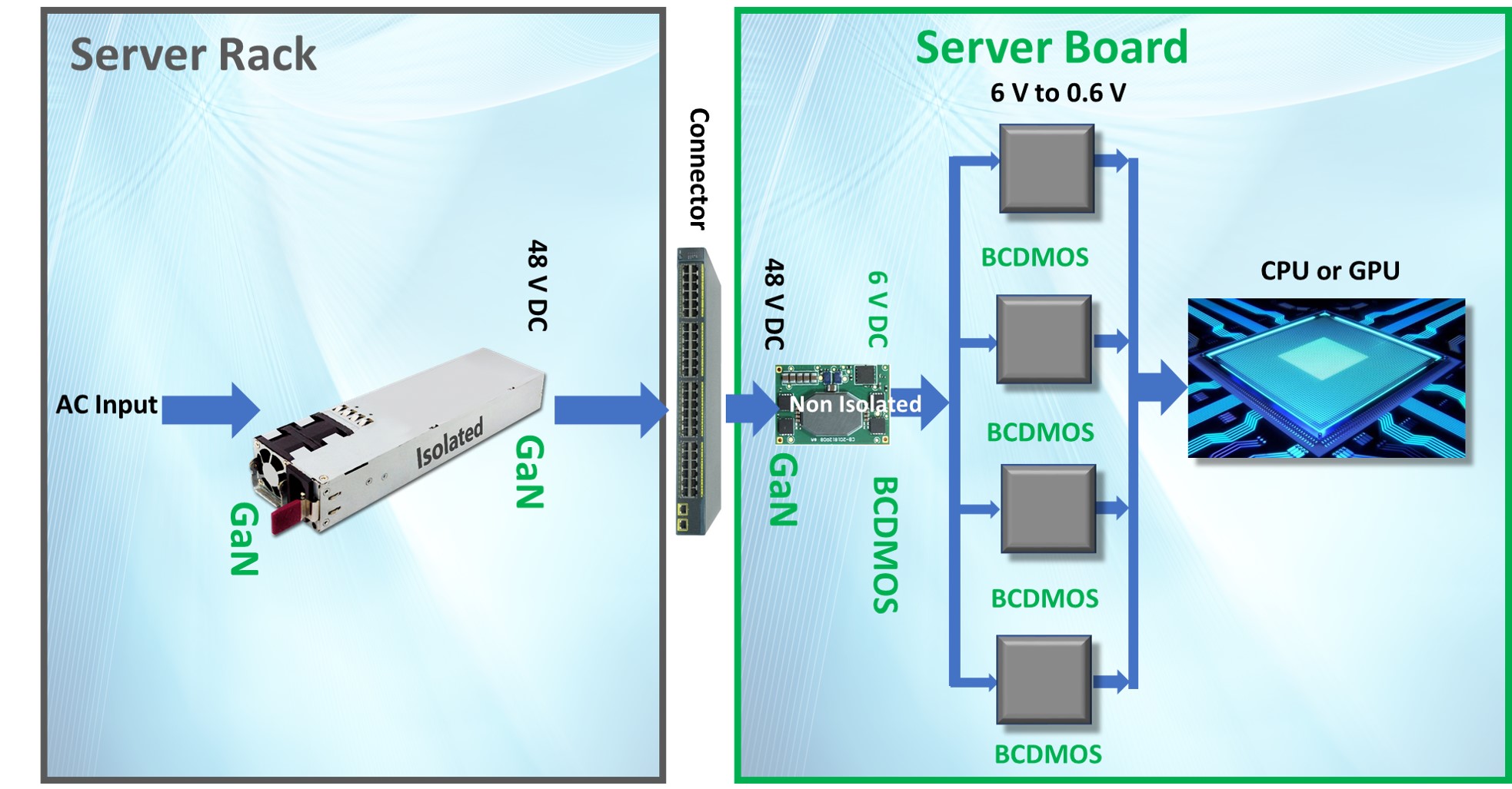
Figure 3: Emerging 48 V input server board topology
Due to increasing power, many server designs, especially those adopted by new hyperscale servers and the latest generation of GPU-based AI servers, are migrating from 12V input to 48V input on the server board.
The four times higher input voltage eases the distribution of high power and improves efficiency (Figure 3). The evolution from legacy 12V server racks to 48V racks reduces energy losses by over 30%.
Additional key system-level benefits for 48V in-rack distribution topologies are copper utilisation and distribution losses. Additionally, for a given power level and bus cross section, 48 V systems reduce distribution bus losses by 94% compared to 12V designs. In other words, a 48V distribution bus can deliver four times the power of a 12V system with the same bus loss.
Intermediate bus architecture
The most efficient way to convert power from 48V to PoL is a two-stage conversion, with intermediate voltage of 12V or 5.0V. By going to a 5V intermediate bus, there are some additional benefits over a 12V bus.
By lowering the intermediate bus voltage to 5.0V, a change in technology from power MOSFETs for the PoL converter to higher density BCDMOS power stages can occur. BCDMOS power stages can go to higher frequencies making the PoLs smaller and allowing the PoLs to be placed much closer to the GPU or CPU.
This reduction in distance can reduce the resistance between the PoL and the GPU/CPU by as much as 350µΩ. At 1000 A, that is a 350W reduction in losses!
There are multiple topology solutions for a 48V to 5.0V intermediate bus. LLC topology, however, offers the best system efficiency and very high power density. There are small (486mm2) 300W modules reaching 1700W/in3on the market today, and a 600W, 936mm2 module available for evaluation. All three of these high-power density modules are made possible by 100V, commercially available GaN devices that enable 1MHz operations.
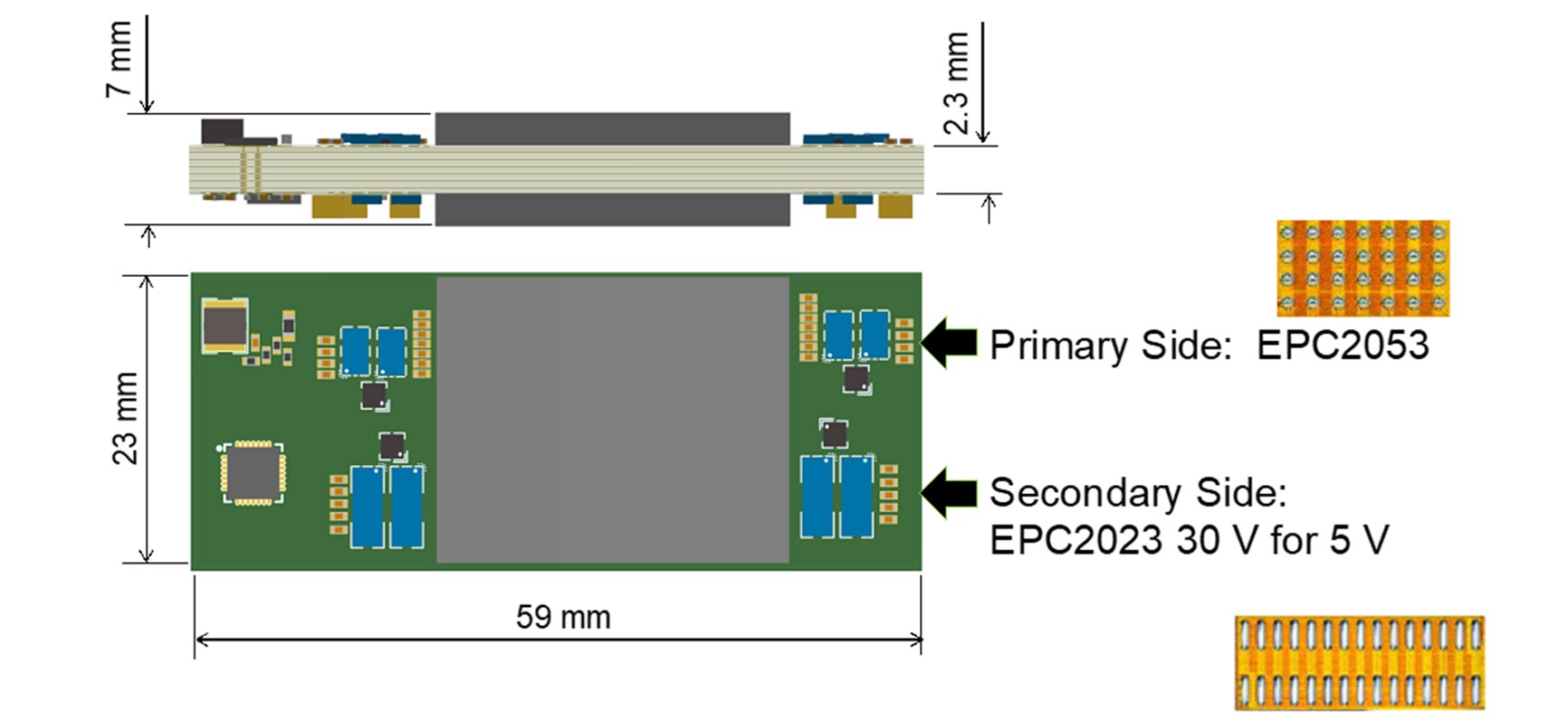
Figure 4 shows a 1kW LLC solution in a 1/8th brick size and projected full load efficiency of 98%.
The latest server applications require >2kW input power for a 48V server and up to 1kW for an AI board. Using 1kW modules reduces the number of modules to optimise overall system size and cost.

Figure 4: 1kW LLC solution in less than 1/8th brick
48V topologies
There are three common converter topologies used for 48V conversion in servers to either 12V or down to 5.0V:buck converter, LLC and switched capacitor.
The switched cap is inexpensive and very efficient at 48V to 12V at less than 600W, but this topology has limitation for higher power, and it is too complicated for 48V to 5.0V.
The buck is the least expensive and smallest solution for 48V to 12V up to 300W. Both the buck and LLC have higher power density than the switched capacitor. The LLC design allows the best efficiency for greater than 600W for both 48V to 12V and 48V to 5.0V. It also has the best topology for Vin/Vout ratio of 8:1 or 10:1.
Since GaN is a lateral device, it is very easy to integrate solutions beyond discrete devices. Fully integrated power stages have been on the commercial market since early 2020.
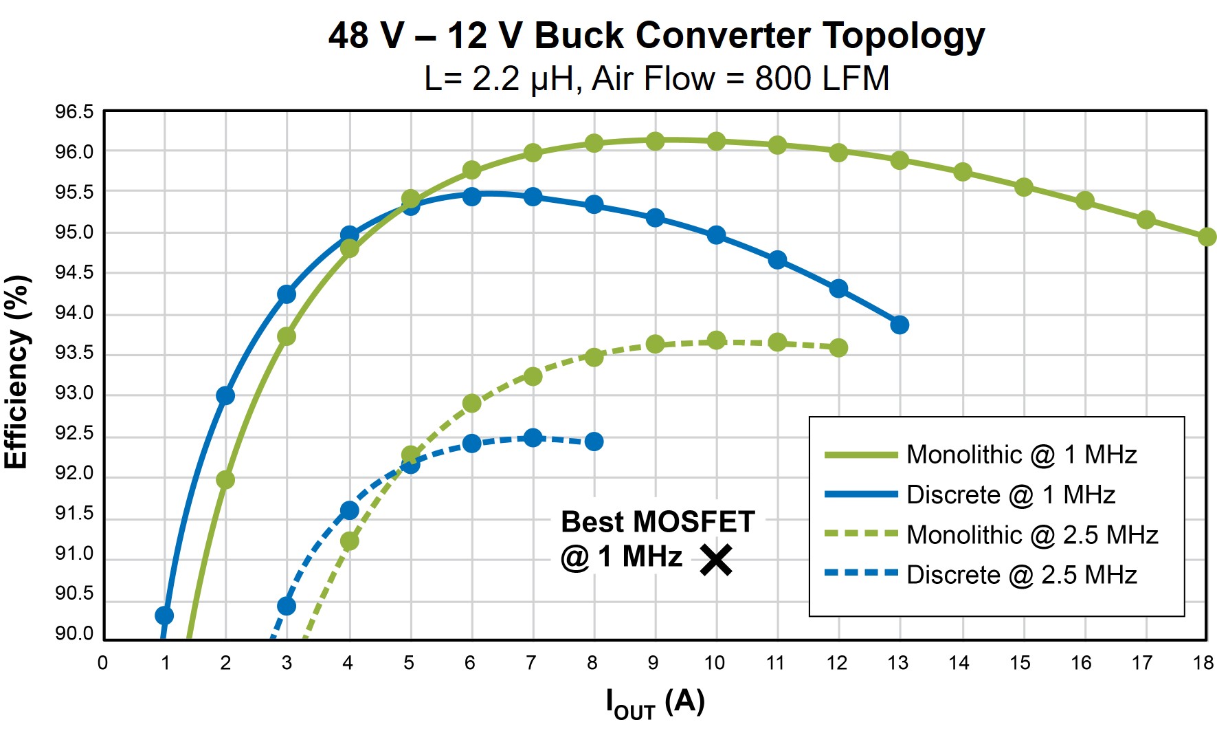
The level of integration improves efficiency. Figure 5 shows the efficiency gain between the integrated GaN power stage and a discrete solution with one driver and two GaN FETs operating at both 1.0MHz and 2.5MHz. The green curves are the integrated solutions and the blue curves are the discrete solutions.

Figure 5: Monolithic vs discrete buck converter topologies
For 48V to 12V at 1.0MHz, the integrated solution delivers greater than 96% peak efficiency and up to 2% efficiency improvement at 12.5A. This improvement can be explained by three factors: the matching of drivers with FETs, no parasitic gate loop, common source and power loop inductances and the thermal balancing of the two FETs. This level of integration also enables space and power loss improvements in the LLC converters.
Conclusion
The requirements for higher power density have increased each year since power MOSFETs were first launched in the late 1970s, and show no signs of slowing down. Artificial intelligence, machine learning, and cloud computing are the applications that are leading the conversion from on-board 12V distribution buses to a two-stage solution where the first stage is 48V, and the second stage ranges from 12V to 5.0V. The 48V input is rapidly shifting from silicon-based power MOSFETs to GaN power transistors, and soon, GaN-based power ICs.
The secondary side, if at 12V, remains the realm of the power MOSFET. As the secondary side migrates to lower voltages, monolithic BCDMOS ICs can serve as synchronous rectifiers at lower cost and higher efficiency than discrete MOSFETs. Similarly, as the secondary bus voltage shifts from 12V to 5.0V, the PoL converter is also shifting towards monolithic BCDMOS power stages that can operate at higher efficiency and at higher frequencies that the aging power MOSFET.
About the author: Alex Lidow is CEO and co-founder of Efficient Power Conversion (EPC)


