The art of DRAM module testing
DRAM technology is well known and components are fully standardised products, which are manufactured with low cost materials and assembly lines. So why are there differences in quality and price anyway?
By Ulrich Brandt, Head of Business Unit DRAM Products at Swissbit AG.
To assure quality, DRAMs are tested multiple times. Some DRAMs see special additional tests, while others receive a reduced test flow. This defines if a component is suitable for industrial, automotive or consumer use. But even if you buy top quality DRAMs from the manufacturer, there is still a handicap to produce top quality modules.
Exposing the DRAM component to the high temperatures of a solder process causes a lot of stress to the cell capacitor and its dielectric. The cell capacitance and retention time of the DRAM typically degrades during the assembly process.
There are always some weak cells which pass the outgoing test at the DRAM manufacturer and degrade during assembly of the module. These cells have a reduced storage capability and fail when operated at high temperature and with disturbing write and read patterns.
To verify that no damage has been done to the DRAM components you need to perform quite powerful tests on module level at the specified maximum operating temperature corners or beyond, if you test with guard band.
For DRAM components the operation conditions are given as min and max case temperatures. This is 0 to 85°C by default, and -40 to +95°C for industrial operation. At low temperatures there are mainly internal contacts failing. At high temperatures the cell retention time is the critical parameter. The only guarantee to verify the full functionality of the DRAM cell after assembly is to test the module both at high and low temperature.
There are two different approaches to module testing: dedicated DRAM testers or application testing.

A module tester has a pattern generator, parametric unit, and driver interface. The pattern generator can create address and data sequences, but is often limited to linear addressing modes. There is no possibility of creating more random sequences. Often the tests are very synthetic and do not resemble the real operation behaviour in a PC system.
This is the strength of motherboard application testing. Failures are relevant, because they occur under conditions that can equally be found during user operation. The disadvantage of pure application testing is the impossibility to change timing settings or I/O voltages.
Above this, there is a more hidden handicap of application testing: The test pattern is run on the same system that incorporates the device under test. First of all you cannot test 100% of the memory area, since the test program and the OS reserve some memory for themselves. But more than that, the CPU has to generate the DRAM test pattern with code written in assembly language. It is not very difficult to write fast patterns that linearly walk through the memory and write and compare. But as soon as you go for complex sequences like random address patterns, using calculation intensive operation code with a lot of XOR operations, the CPU is busy generating the next address, not accessing the memory. You need to distribute the test to multiple threads and cores to increase the band width to the DRAM module, and to test it with critical conditions. Using simultaneous multi-threading in a low level OS like DOS for memory testing is a real challenge and it needs years of experience to write memory test programs that exercise the memory with critical pattern in a short test time.
Another hurdle to overcome in application testing is the support for ECC. This error correction can detect and correct single bit errors of memory modules, an additional security against bit fails and data loss.
In a motherboard that supports ECC, the memory controller permanently corrects all single bit errors that occur during testing, effectively hiding all fails from the test program. The test will report ‘pass’ although the memory module had bit errors, rending the ECC worthless.
You need to implement support for the chipset ECC generator into your memory testing code in order to detect corrected errors and flag the module as fail.
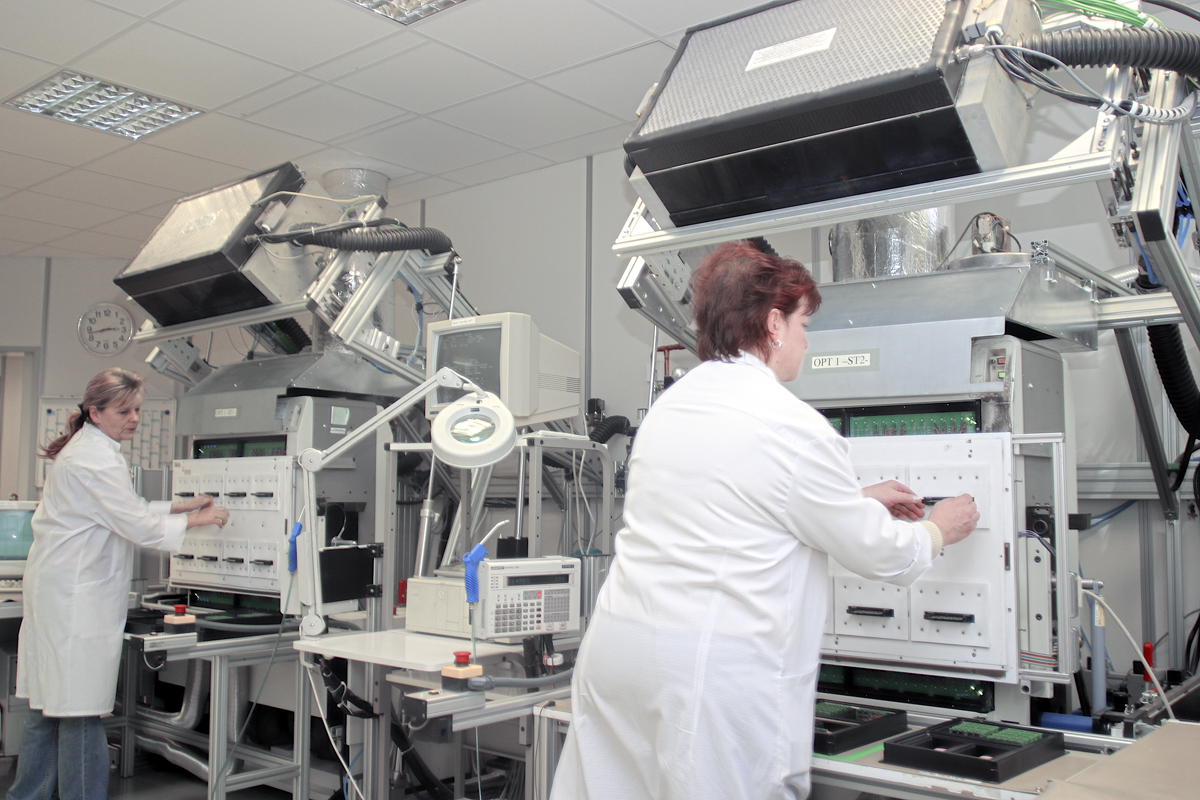
Swissbit combines all of the best of these variables in their module testing. Each module is first tested on a dedicated memory tester, varying timings and I/O voltages and measuring leakage. Then, each module is tested on a main board with a high performance proprietary memory test that causes maximum cell disturbance and long access pauses. For modules with industrial temperature grade, Swissbit tests each individual module at -40°C and higher than +95°C to cover insufficient testing by the DRAM manufacturer and the degradation during the assembly process. In doing so, Swissbit guarantees highest quality, which makes a big difference to modules that have just seen a quick test after assembly.


