The power of low noise in IoT smart sensors
Performance vs. power dissipation - it’s one of the most delicate trade-offs for those who develop smart sensors for the emerging IoT-based application space.
Within the broad spectrum of 'performance', noise is often an important attribute to evaluate, as it can constrain component selection for key functional blocks in a smart sensor, which in turn can increase the power burden.
In addition, noise behaviors can drive filtering requirements, potentially influencing the sensor’s responsiveness to rapid changes in conditions and extend the time it takes to develop a quality measurement.
In applications that support continuous observation (sampling, processing, communication), system architects often have to work through an adversarial relationship between noise and power. Typically, the lowest noise solutions are rarely the ones that also offer the lowest power (within a particular functional class of devices).
For example, MEMS accelerometers commonly serve as a core sensor in remote tilt-measurement systems. The table captures the highlights from two different products that offer high performance in either noise or power at this time: the ADXL355 (low noise) and ADXL362 (low power) from Analog Devices.
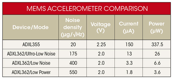
Three of the four entries in the table represent selectable modes of operation in the ADXL362, while the fourth entry represents the key metrics for the ADXL355. Starting with the key boundaries of this trade space, the ADXL355 offers nearly 27 times lower noise than the lowest power mode in the ADXL362, but at much higher power dissipation. For an application that has more challenging performance requirements, which may require consideration of the highest performance mode in the ADXL362, the ADXL355’s noise will be nine times lower, while the ADXL362’s power dissipation will be 13 times lower.
When supporting an application that will not require continuous observation and measurements, the relationship between average power dissipation and noise gets more interesting. The relationship between noise and power dissipation can even become complementary, which may seem somewhat surprising for some.
For others, however, this is great news, as previous generation designs may have been delayed while developers struggled to determine if power or performance should drive their designs. Now, rather than waiting for someone else to answer to that same old question, smart sensor architects are pressing to redefine their own work by quantifying relevant options within this trade space, on their own.
Smart-Sensor architecture
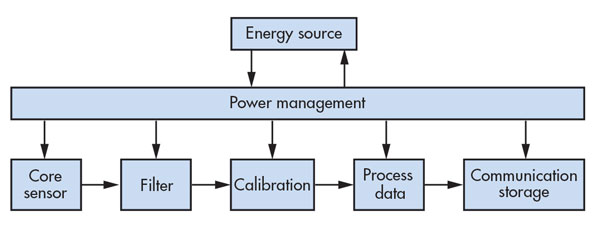
Quantifying relevant options for a particular application starts with making some assumptions about the signal chain, so that this can start with a conceptual architecture. Figure 1 provides a generic example of a smart sensor’s architecture, which contains the most common functions:
Core sensor
The signal chain in a smart-sensor node starts with the core sensor function. In its most basic form, the core sensor is also known as a transducer, which translates a physical condition or property into a representative electrical signal. A transducer’s scale factor describes the linear portion of its electrical response to the physical property or condition that it’s monitoring. For example, a temperature sensor with an analog output, such as the AD590, will offer a scale factor in units of mV/°C. A digital accelerometer, such as the ADXL355, will offers its scale factor in terms of LSBs/g or codes/g.
Filter
The next functional block in the signal chain is the filter. The purpose of this stage is to reduce noise from frequency bands that the core sensor may support, but aren’t relevant in the application. In a vibration-monitoring application, this may be a bandpass filter that separates random vibration from a specific spectral signature that can indicate degradation of a machine’s health. In a tilt sensor, this can be a simple lowpass filter, such as a running average. In this case, the length of time presents an important tradeoff between the settling time and residual noise in the filter’s output.
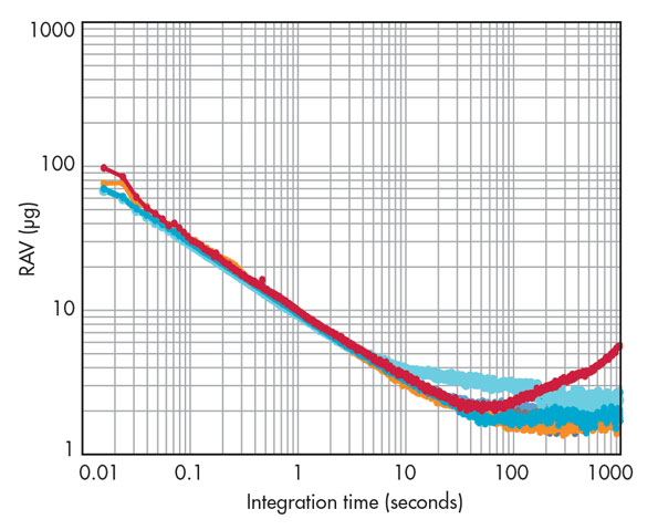
Figure 2 offers an example of an Allan Variance curve for the ADXL355, which presents the uncertainty (noise) of a measurement, with respect to the averaging time that produces that measurement.
Calibration
The purpose of the calibration function is to improve the precision of the measurement, through application of correction formulas. In the most demanding applications, these correction formulas typically come from direct observation of sensor responses, while they’re measuring tightly controlled conditions. For example, in a tilt-sensor application, the calibration process will involve observation of the MEMS accelerometer’s output in several different orientations, with respect to gravity.
The general objective of these observations will be to observe the sensor response to enough orientations to resolve all 12 correction factors (M11, M12, M13, M21, M22, M23, M31, M32, M33, bx, by, bz) in the following relationship:

The correction factors in Equation 1 address bias, sensitivity, and alignment errors. This formula can also expand to account for higher-order sensor behaviors (nonlinearity) or environmental dependencies (temperature, supply level).
Data processing
The data processing function translates calibrated and filtered sensor data into a measurement result that best supports the application. In a vibration-monitoring system, this could be a simple root mean square (RMS)-to-dc conversion or a fast Fourier transform (FFT) with spectral alarms (see ADIS16228). In a tilt-sensing application, the smart sensor will translate acceleration-based responses to gravity into orientation angle estimates, using Equations 2, 3 or 4:
![]()


These three relationships represent tilt estimation with one, two, and three accelerometer measurements, respectively, assuming perfect orthogonality between each of the accelerometers.
Communication/storage
The communication/storage function supports data staging and connectivity with all IoT cloud services (encryption/security, storage, and analytics).
Power-Cycling Operation
The power-management (PM) function provides three different functions for a typical smart sensor. The PM’s first function is to manage all of the power-sequencing requirements for all components in the signal chain. The PM’s second function is to convert the supply from the Energy Source into voltage(s) that support optimal operation in all of the components in the signal chain. Finally, in systems that have regular measurement intervals, the PM system provides scheduling to trigger each measurement event.
Power cycling is common way to identify this type of discontinuous operation in a smart-sensor node. By resting in a low-power (or zero power) state, in between measurement events, this technique helps conserve energy in the smart sensor. Figure 3 illustrates the instantaneous power dissipation over a complete measurement cycle for a smart sensor that’s leveraging this technique.
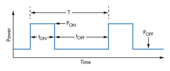
Equation 5 provides a simple relationship for estimating the average power dissipation (PAV), using the operational attributes from Fig. 3:
where:
• PON is the average power dissipation in the smart-sensor node when it’s sampling and processing data to produce and communicate a relevant measurement result.
• POFF is the average power dissipation that the smart-sensor node requires to support its low-power “sleep” mode.
• tON is the time that it takes the smart sensor to turn on, produce a measurement result, communicate that result to the IoT cloud, and turn back off.
• tOFF is the time that the smart sensor is dormant (sleep mode or completely powered off).
• T is the average measurement cycle time.
Measurement Process
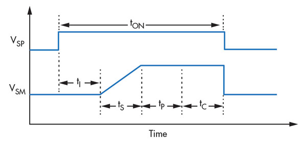
During its on time (tON), a smart sensor will typically work through several different operational states. Figure 4, along with Equation 6, offers an example sequence, which breaks the on time down into four different segments: initialisation, settling, processing, and communication.
where:
• tI is the initialization time, which represents the time between power application (VSP) and the time when each component in the signal chain is ready to support data sampling and processing.
• tS is the settling time, which represents the time between the first data sample and the time that the filter’s output (VSM) has settled to a sufficient level of accuracy.
• tP is the processing time, which represents the time it takes to produce the measurement result, after the filter settles. This can include application of calibration formulas, application-specific signal processing, and data encryption for the IoT security protocol.
• tC is the communication time, which represents the time it takes to connect with the cloud services, transmit the encrypted data, and support any error checking or authentication services.
Settling-Time Influence
Using the segmentation of the different phases in a measurement cycle (Fig. 4 again), the settling time of the filter is an obvious area where noise can influence the power dissipation in a power-cycling, smart-sensor node.
In general, the decrease in noise magnitude that comes from averaging is proportional to the square root of the averaging time, while the increase in energy consumption is directly proportional to the averaging time. Therefore, reducing the noise magnitude by a factor of 10 will cause the energy consumption (during filter settling) to increase by a factor of 100! This type of disproportional tradeoff can quickly favor the sensor that requires the least amount of filtering (lowest noise).
Application Example
Consider the microwave antenna platform in Figure 5, which rests on a tower platform. In this type of communication system, the reliability of the data link depends on the accuracy of the pointing angle. Maintaining the pointing angle can require manual adjustment, especially after earthquakes and other disturbances to the platforms that these antennas rest on.
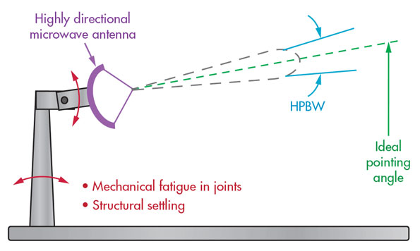
This type of remote maintenance can be costly and limited in response time. Consequently, one antenna operator is investigating the feasibility of using MEMS accelerometers to monitor changes in orientation of the antenna body as part of their maintenance response strategy.
The system architect starts this investigation with their most basic functional requirement: maintain reliable communications on each antenna platform. In this system reliable data communications requires that the antenna’s pointing angle must stay within the antenna’s half-power beam width (HPBW) (Fig. 5, again) at all times. Therefore, they determine that they would like to trigger a maintenance visit when the antenna’s orientation changes by 25% of the antenna’s HPBW, over a short period of time.
Within the error budget for supporting this goal, the architect allows for the peak noise in the tilt measurement to be 10% of the measurement objective (25% of HPBW). For simplicity, the architect also assigns the peak value of the noise to be equal to three times greater than the RMS value of the noise. Equation 7 captures all of these defining inputs and simplifies it into one relationship, which simply states that noise in the tilt measurement needs to be 120 times lower than the HPBW.

In order to relate this angle noise requirement to the same performance metric in the MEMS accelerometer, Equation 8 comes from plugging the result of Equation 7 into the basic accelerometer to tilt formula in Equation 2.

So, for an antenna that has a HPBW of 0.7 degrees, the noise in the accelerometer must be less than 100 μg to meet the existing criteria:

This result establishes a metric to use in determining the amount of averaging time that each candidate sensor (see table) would need, in order to achieve 100 μg of uncertainty in a measurement. Reviewing Fig. 2 reveals that the ADXL355 will require an averaging time of ~0.01 seconds (tS355 = 0.01; Equation 10) to get below this level.

For a quick approximation, one can assume that since the ADXL362’s noise is nine times greater than the ADXL355, it will require an averaging time that is 81 times that of the ADXL355 (tS362 = 81 x tS355; Equation 11), in order to reach the same objective. Equation 10 captures the energy consumption that comes from the settling time in the ADXL355, and Equation 11 captures the energy consumption that comes from the settling time of the ADXL362 (see table).

Ironically, the lowest energy consumption for this level of noise performance comes from using the lowest-noise accelerometer, not the lowest power accelerometer! Equation 12 divides the energy estimates for each sensor in Equations 10 and 11, by the measurement interval (T = 10 seconds), in order to estimate the settling time’s contribution to power dissipation.

Conclusion
This particular discussion has revealed a specific scenario, where the lowest power solution came from using the core sensor with the lowest noise, not the one that provides the lowest power dissipation. For those developing smart-sensor concepts for an emerging class of IoT applications, which have demanding performance requirements and limited access to energy sources, this type of solution path could present an important lesson.
In essence, clever solutions may be available for those who are willing to first understand, then challenge even the most fundamental paradigms. Sometimes, the best performance and the lowest power dissipation could actually come from the same sensor.


