
The last piece of the puzzle
Thanks to a new process, a CMOS RF power amplifier has matched the performance of GaAs devices for the first time, resulting in new possibilities for reconfigurable RF front ends, reports Sally Ward-Foxton.
The widely-adopted compound semiconductor Gallium Arsenide (GaAs) may be about to lose its stronghold on the RF power amplifier (PA) business. A new RF SOI process from Peregrine Semiconductor has enabled the company to produce a silicon CMOS PA with equivalent performance to its GaAs counterparts. Although CMOS PAs have been available for some time, their performance was lacking and in the highly competitive smartphone market it wasn’t good enough to gain any market share.
![]()
Figure 1: Comparing CMOS and GaAs PA power-added efficiency performance without Envelope Tracking (ET). Peregrine is claiming equal performance for GaAs devices and the PA from its CMOS platform, Global 1.
The performance of Peregrine’s new CMOS PA, part of its Global 1 CMOS RF front end system, is shown in Figure 1. Power-added efficiency, a standard industry metric for PA performance when measured for a WCDMA signal with an adjacent channel leakage ratio (ACLR) of -38dBc, is equal for the GaAs PA and Peregrine’s device at close to 50%. The nearest competing CMOS device falls 10 percentage points short. The data in Figure 1 was gathered without envelope tracking (ET) or digital predistortion, but when ET is added, the PAE for Peregrine’s PA increases up to 20 percentage points.
Long time coming
The CMOS PA owes its performance to a process unveiled by Peregrine last Autumn – UltraCMOS 10. An UltraCMOS 10 wafer can be seen in Figure 2. This advanced process has been a long time in the making.
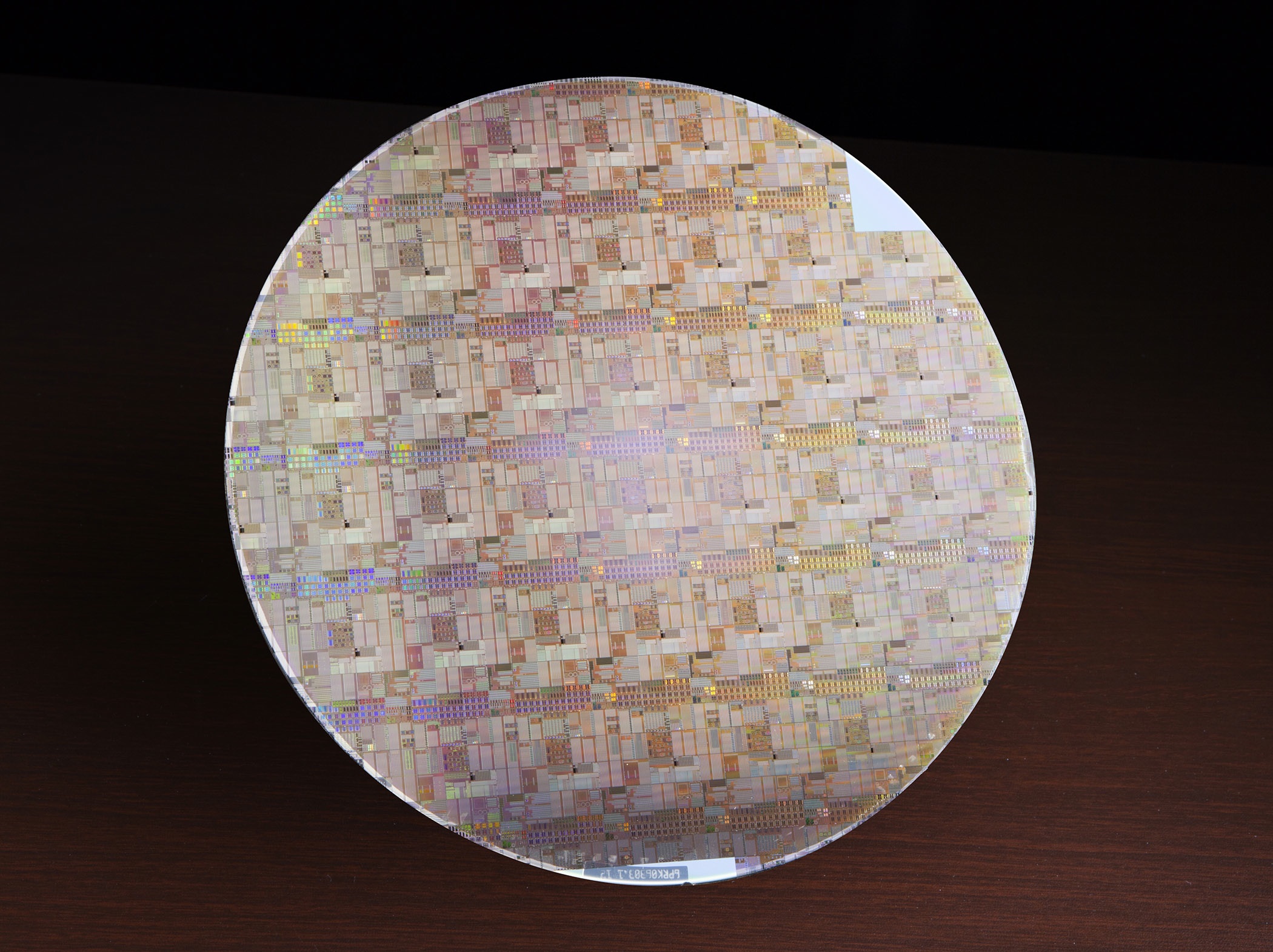
Figure 2: An UltraCMOS 10 wafer. Peregrine worked with Globalfoundries and Soitec to develop this CMOS process that can rival GaAs for RF power amplifiers.
“Peregrine has worked for the last 25 years on SOI technology platforms. We describe it as a technology platform because we combine process developments with circuit level IP and advanced substrates,” says Duncan Pilgrim, Director of Technical Marketing at Peregrine. “Until UltraCMOS 10, Peregrine used a Sapphire substrate due to its near perfect RF properties. We worked with Globalfoundries and SOITEC to develop UltraCMOS 10 which for the first time makes use of a CMOS based SOI substrate and a 130nm process node.”
A primary challenge with a standard CMOS process is the breakdown voltage of the FETs. Most CMOS PA companies have solved this by using power combining techniques at the output in order to minimise the voltages across the FETs.
“This power combiner is lossy and causes significant degradation in efficiency,” says Pilgrim. “Peregrine approaches the problem very differently and uses stacking techniques to create a virtual HBT [Heterojunction Bipolar Transistor] device which enables a similar architecture to ones used in GaAs power amplifiers.”
The RF transistors created by UltraCMOS 10 feature a strikingly low RON*COFF, the figure of merit for RF switches. Figure 3 tracks the progress made on RON*COFF over the last 8 years. According to Pilgrim, this reduction is in large part due to the shift to the new process node of 130nm.
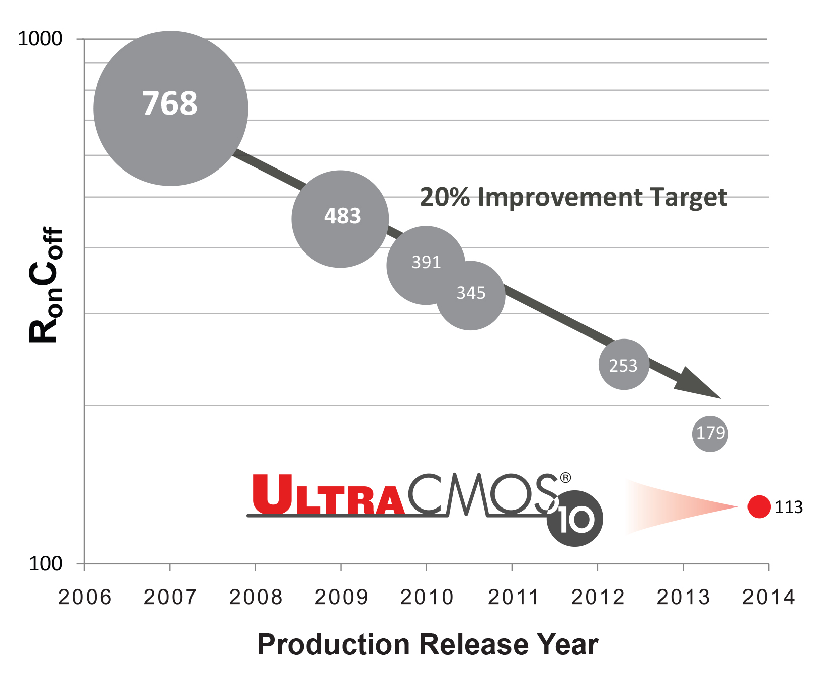
Figure 3: The reduction in RON*COFF over the years has been steady, but the shift to a smaller process node has placed UltraCMOS 10 ahead of the curve.
All-CMOS RF
The new PA is part of Global 1, Peregrine’s all-CMOS RF front end. Global 1 includes a 3-path multi-mode multi-band PA, post PA switching, antenna switch and antenna tuner. Because all these blocks are now CMOS, they can be integrated at die level onto the same chip.
The implications of this technology development are pretty compelling. To start with, eliminating GaAs means the well-established CMOS supply chain can be used to deliver higher volumes at lower cost, with guaranteed repeatability. There is also a roadmap to more advanced process nodes and increased wafer sizes.
Because all the blocks of the CMOS RF front end are now CMOS, higher levels of integration are possible, as demonstrated by Global 1. Previously, RF front ends containing GaAs PAs had to use multi-chip module packaging. This high level of integration in turn allows a greater degree of reconfigurability, a huge bonus when set against an evolving RF landscape which is placing more and more demands on the RF front end.
“To increase the data throughput LTE uses a complex transmit modulation scheme [SC-FDMA], this means that higher linearity is required to optimise the transmit path,” Pilgrim explains. “There are no global frequency bands for LTE so there has been a massive proliferation of frequency bands in order to support a global footprint. In addition, the increase in data rates means that even at the regional level more spectrum is required to support this growth. In many cases the spectrum that is being rolled out has resulted in more complex interference scenarios, which is being further compounded by the roll out of carrier aggregation.”
To keep up with demands for more data, there are now more than 40 frequency bands worldwide for LTE, and more than a 5,000-fold increase in the possible number of operating states is forecast for the next few years (the product of the number of frequency bands, modulation schemes, power amplifier modes, antenna tuning states and downlink carrier aggregation). This means that RF front ends are having to become much more complex to keep up. A reconfigurable RF front end would certainly help keep things simple.
“Reconfigurability removes the need for a soldering iron and bag of capacitors!” Pilgrim says. “Instead of manually retuning the power amplifiers for the supported frequency bands Global 1 can be electrically reconfigured, this means that it is fast and simple to change the supported frequency bands and to optimise the interface between the duplexer and the power amplifier, which can take out any variances due to trace length and loss.”
“This just scratches the surface of what reconfigurability can enable,” he adds.
In fact, there is a huge benefit to smartphone makers in the ability to reduce inventory. As an example, the Apple iPhone 5S launched with five handsets for the different regions with differing RF front ends (and which were otherwise identical). If the RF front end could have been common to these models, there would be potential cost savings in engineering, validation, manufacturing and supplier and inventory management. Pilgrim says that when truly global handsets arrive, they will be configured in the factory, based on the specific bands supported, and also reconfigured in the field based on the mode of operation (i.e., WCDMA or LRE, downlink carrier aggregation, etc.).
A reconfigurable RF front end is the final piece of the puzzle - basebands and transceivers have effectively been software defined for a number of years. The synergies created by having entirely reconfigurable hardware are now open to OEMs, and that should result in cost savings for development and deployment of new smartphone products.

Featured products

MAX17793
Analog Devices Inc.

3V to 80V, 3A, High-Efficiency, Synchronous Step-Down DC-DC Converter
| SKU: | MAX17793 |
|---|---|
| Stock: | 9316 |
| Cost: | $3.64 |

MAX22516
Analog Devices Inc.

IO-Link Data Link Controller with Transceiver and Integrated DC-DC
| SKU: | MAX22516 |
|---|---|
| Stock: | 8000 |
| Cost: | $5.42 |
Product Spotlight
102991834
BeagleBoard

Single Board Computer (SBC), BeagleY-AI
AM67A BeagleY-AI Jacinto 7 AR...
| SKU: | 2820-102991834-ND |
|---|---|
| Stock: | 208 |
| Cost: | $56.24 |
SC1110
Raspberry Pi

Raspberry Pi 5 2GB
The Raspberry Pi 5 2GB model represents a leap for...
| SKU: | 2648-SC1110-ND |
|---|---|
| Stock: | 0 |
| Cost: | $38.33 |
AKX00069
Arduino

Arduino Plug and Make Kit
The Arduino Plug and Make Kit features the ...
| SKU: | |
|---|---|
| Stock: | 968 |
| Cost: | $66.97 |
300361-0011
Molex

MX150 Mid-Voltage MatSealed Female Connector Assembly, Dual Row, 20 Circ...
| SKU: | |
|---|---|
| Stock: | 280 |
| Cost: | $2.51 |