Pre-layout work and good signal integrity simulation
Digital signals controls all the devices today. A failure in signal integrity simulation creates unwanted phenomena like sudden freeze of the device or unknown software errors. These happens when the digital signal gets corrupted during transmission. How the device survives from these depends on used error correction and software self-monitoring. Matti Uusimäki, Key Account Manager, Radientum further explores.
Signal integrity simulation analysis after layout design is too late. The proper phase to start is prior to the layout work. We call that work pre-layout signal integrity analysis. It can be split into two main areas. Analysing the signal path elements effect to signal and analysis of possible cross talk.
The signal path is the most important because it has a direct effect to signal. It is good to remember that making the signal path barely to match demands is not enough. If there is no noise margin the crosstalk or noise coupling can happen often and be harmful.
With proper pre-layout signal integrity simulations, the critical design details can be checked prior to the layout work and a guide to layout designer is created. This work can overlap into the actual layout design phase if there is a case where the guide cannot be followed, and new ideas and instructions are needed.
When signal integrity simulations are done prior to layout work, signal integrity of signals is actually designed. If you only measure afterwards the signal eye-diagram, you just conclude what came out. In the worst case the signal starts and stops under the component and travels inside the layers and measurements are not even possible, simulations are the only way then.
Pre-layout simulation
In pre-layout phase of signal integrity work, the design outlines and known critical details are analysed and simulated to create a design guideline.

The first step is to define the PCB stack-up. What kind of vias are used and what are the signal layers and ground layers for return currents of signals. In Figure 1 there are three examples seen in the industry, all of them has different effects to signal impedances.
Vias and discontinuities in signal integrity simulation
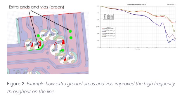
Vias are the typical point of impedance discontinuity when jumping from layer to another. In Figure 2 there is an example how the ground fills and ground vias close to signal vias are affecting. On the right-hand side, you can see how the additional grounds improves the high frequency performance with less high frequency attenuation on the signal path. This improves the very fast digital signals eye diagram.
This LinkedIn video has a nice video of signal integrity simulation presenting the via back drill effect to signal eye. For efficient pre-layout work, the Figure 2 right hand side frequency domain results give enough information already to select proper layout approach.
The impedance of a signal via depends strongly where is the nearest ground via and is it connected to the proper ground layer for return current point of view. For example, the Figure 2 improvement comes strongly due to more stable impedance over the signal path. Two vias of a differential signal needs a balance against each other and to the ground vias next to them for proper impedance. Other places to look in more detail are under the components and connectors or any other ‘not straight line’ places on the board.
Cross talk in signal integrity simulation
If the signal shape is not ideal, it is typically generating more radiation and that is bad for other signals. The cross talk to other lines happens more easily if there is, for example, overshoot on the signal. In cross talk point of view, it is important to look how the signals are routed compared to each other. Long parallel lines are known areas of crosstalk and proper grouping of the signal is the key for success. Another key is a solid ground connection between the components. Sometimes signal vias are breaking the ground layer badly causing poor return path for the signal.
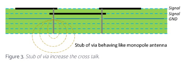
One overlooked section for cross talk are the signal vias. They can be a point of signal line mismatch and point of in-board cross talk. As an example, there has been a case where the through hole via was used in jump from layer 1 to 2 and the remaining stub of via (layer 3-6) has been acting like a radiator. This stub increases a cross talk and causes impedance mismatch on the line itself. The mismatch causes reflections on the line reducing the clarity of the signal eye and possible crosstalk reduces it even more. With signal integrity simulations you can decide is the expensive back drilling necessary or not.
These examples give an idea how to use 3D electromagnetic simulations in pre-layout signal integrity work. More details can be analysed depending on the used solutions or topology of the layout. Radientum can provide these simulations as a service in various scopes, from specified challenge areas to comprehensive simulations of the entire device.
Disclaimer: The views and opinions expressed in this article are those of the author. It is intended only as a sharing of antenna design knowledge for educational purposes.


