Meeting today’s design requirements, regardless of experience
Many of today’s electronic systems involve multiple circuit boards. Furthermore, many of these systems use multiple interfaces of different types - like I2C, I2S, and GPIO - to collect data from peripherals and sensors and to communicate this data between boards.
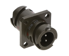
In addition to the fact that routing signals through congested boards and connectors can present its own challenges, circuit board real estate is often at a premium, as is the space within the system’s enclosure. In addition to increasing cost and taking up space, connectors are often the most unreliable components in the system.
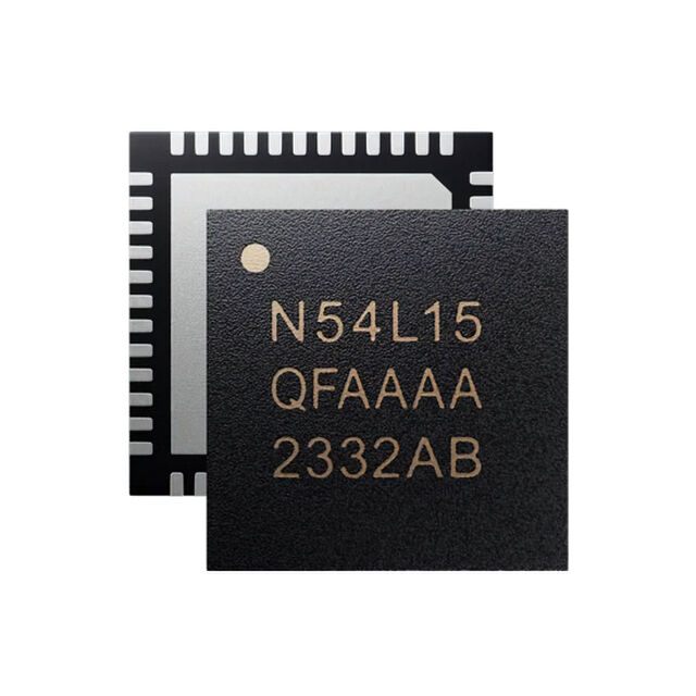
Lattice Semiconductor has developed an innovative new way for system architects and developers to use tiny, low-cost FPGAs to dramatically reduce the number of board-to-board xd and module-to-module connectors, thereby increasing the reliability of the system while also reducing its size and cost.
This solution can be customised by developers with FPGA design experience. Even better, it can be quickly and easily deployed by developers with no FPGA experience whatsoever. Making Good (or Bad) Connections The vast majority of today’s electronic systems involve two or more circuit boards and/or modules. (For the remainder of this paper, unless otherwise stated, the term ‘circuit boards’ or ‘boards’ will be assumed to encompass ‘modules’).
In parallel Lattice Semiconductor has also published a whitepaper: ‘FPGA-Based Single Wire Aggregation (SWA) for FPGA and Non-FPGA Designers’ which can be downloaded above.


