Surface imaging and metrology software solution for analysis
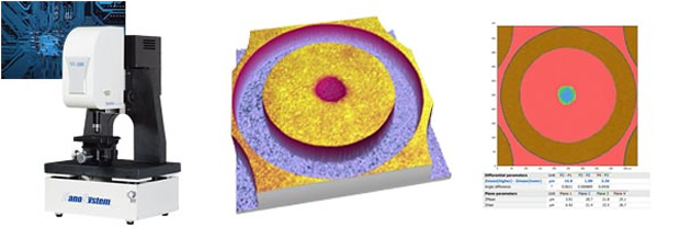
The release of NanoMap Alpha software based on Digital Surf’s industry-standard Mountains software platform has been announced by Nanosystem. NanoMap Alpha is now integrated into the company’s NV- and NVM-series high precision 3D optical measurement systems, thus providing an ideal solution for analysing semiconductors, PCBs, displays, engineered parts, chemical materials, optical parts etc.

Image: Contact pad analysis using NanoAlpha Map: sample visualisation in 3D & automatic step height analysis.
“NanoMap Alpha software makes it easy and intuitive to measure a wide variety of surface materials and parameters ,” stated Michael Yang, Director of Nanosystem “With its built-in automation features, it will greatly enhance our customer’s experience and make significant improvements to manufacturing productivity.”
“We are proud to accompany Nanosystem in its mission to support operators, engineers and researchers worldwide working in surface measurement and inspection” said Christophe Mignot, Digital Surf CEO. “Mountains Technology has once again strengthened its position as the tool of choice for surface imaging and analysis.”
Features include:
- Ease-of-use: User-friendly ribbon interface and contextual tabs with intuitive icon-based tools
- Productivity: Quick & easy report generation - Analysis routines can be saved as templates and re-applied to batches.
- Flexibility: Each analysis step can be fine-tuned at any time, all dependent steps are automatically recalculated.
- Compliance with the ISO and national standards: Analysis of surface texture, roughness, waviness, flatness, grains etc.
- Surface geometry analysis - including volume of surface structures (bumps, holes), step heights, contour etc.
- And also: Comprehensive built-in user help - Software available in 11 languages (EN, FR, DE, ES, IT, PL, PT-BR, CN, JP, KR, RU)


