Ultra-thin is the new bulk
The quest for smaller, faster, cheaper integrated devices really drives the semiconductor industry from a commercial point of view; an ever-present burden on developers working on the next great process breakthrough. Philip Ling reports for ES Design magazine.
Fortunately, the timescales involved in developing a process technology aren’t entirely governed by the lifecycle of commercial goods, even if that’s where it will inevitably be deployed.
Silicon-on-Insulator technology is a point in case; it has been in development for many years but is probably still viewed as niche rather than a mainstream process. However, that may change in the near future, with the demonstration of an ultra-wide voltage range (UWVR) DSP based on a 28nm ultra-thin body buried-oxide (UTBB) fully depleted SOI (FD-SOI) technology from STMicroelectronics.
The results of the demonstration were presented recently at the International Solid State Circuits Conference (ISSCC) in San Francisco, the preeminent event for sharing research in the semiconductor industry. “UTBB FD-SOI technology is ST’s faster, cooler and simpler solution,” said Phillippe Magarshack, Executive Vice President, Design Enablement Services at ST. “It delivers significant improvements in performance and power savings, while minimising adjustments to existing deign and manufacturing methodologies.” He went on to say: “This demonstration DSP shows that FD-SOI is blazing the trail for better portable and battery-powered products, using more efficient semiconductor chips, all the way down to the 10nm node.”
Planar process
ST introduced FD-SOI in 2012, describing it as a planar technology that could simplify the manufacturing process thanks to two primary innovations; a ultra-thin insulation layer, and an ultra-thin channel. As the channel contains no dopants it is described as being ‘fully depleted’ and it is the combination of these two breakthroughs that ST terms UTBB, or ultra-thin body and buried oxide.
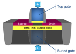
The company’s results shows that the a transistor manufactured in the FD-SOI can operate up to 30% faster than the maximum frequency of an equivalent transistor manufactured using bulk CMOS. This is enabled, in part, by a shorter channel length, but because the ultra-thin insulation layer prevents any leakage to the substrate it allows much more effective body biasing, providing greater control over the channel and two independent gates (Figure 1).

Figure 1: Leakage to the substrate is prevented by the ultra-thin insulation layer
ST also claims that FD-SOI transistors can run extremely fast at low voltages, as shown by the demonstration device presented at ISSCC which is able to operate at 10x ‘state of the art’ frequencies at just 0.4V. While a lower supply voltage can lead to greater energy efficiency, unwanted leakage currents are also contained by the buried oxide layer, which confines the electrons flowing from source to drain, supporting ST’s claims of it being ‘cooler’ than bulk silicon technology.
Crucially, the manufacturing process makes use of the existing fab infrastructure, with the same design rules as bulk planar technologies, meaning that porting an existing design to FD-SOI should be simple. With the 28nm planar UTBB FD-SOI process now in production, a 14nm node is already in development, with a proven scaleability down to 10nm.


