QFN centre pads are so last decade
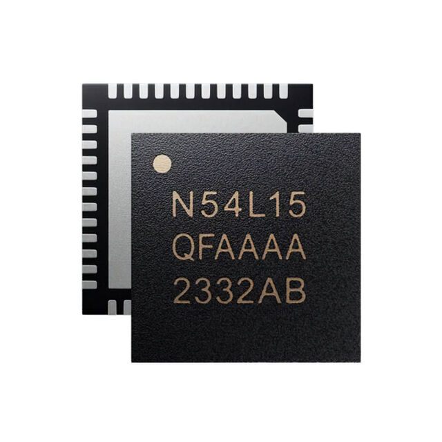
The QFN (quad flat pack, no leads) package can no longer be considered exotic. It was about a decade ago, but not any more. In fact, with the wafer scale BGA, it's one of the more common packages for new chip designs. Not all QFNs come with an exposed metal pad underneath, but most do, and that can still cause problems with reflow solder. The pad itself isn't the problem, but improper solder paste stencil layer design can be.
Author: Duane Benson, Chief Technology Champion, Screaming Circuits
The default stencil layer in the CAD library footprint might have an opening the full size of the metal pad. If that's the case, you'll need to modify the footprint so that you get 50-75% coverage with solder paste.
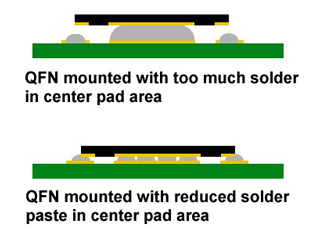 If you don't, you may very well have yield problems. With a 100% open area, you'll most likely end up with too much solder in the middle. The part will ride up or float, and may not connect with all of the pads on the sides of the part.
The first illustration shows a stencil with too large an opening in the centre, a segmented paste layer in the CAD footprint, and the resultant segmented stencil. You may note that I said to shoot for 50-75% coverage and ask: "Well, is it 50 or 75%? What gives?"
True, that is a bit of ambiguity. However, anything in that range should be fine for prototype boards. If you're going for volume production, you'll want to work with your manufacturer to tweak the design for best high volume yield.
Good news on this front is that many QFN manufacturers and parts library creators have taken notice of this. It's far more likely now, than it was ten years ago, to find a datasheet correctly illustrating this, and footprints created correctly. But, always check your footprints to make sure.


