Is SiC key to high power semiconductor technology?
Ewan Ramsay, Principal Engineer, Raytheon UK, explains why SiC (Silicon Carbide) holds the key to high power semiconductor technology and how it can help push electronics further into harsh environments.
Silicon-based components dominate the electronics industry and are an enabling technology for numerous applications. However, all components have operational limits, imposed by the material properties of Silicon, which restrict the extent to which electronics can be used in harsh environments and which restrict the power densities that can be achieved by power semiconductors. Accordingly, alternative materials are needed to extend the use of electronics further into virtually every industrial sector. SiC is one such material, as its properties can allow higher temperature and higher voltage operation, along with higher speed switching, improved power densities and a greater tolerance to radiation.
Conventional Silicon-based device ambient temperature must generally be kept well below 125°C and though technology variants, such as Silicon on Insulator (SoI), can raise the bar by about 100°C, thermal management is an essential requirement for the vast majority of industrial applications. However, thermal management adds considerable weight to conventional electronics systems, and in the aerospace and automotive sectors - where electrical powered systems are increasingly replacing those which have historically employed hydraulics or pneumatics - this is very much at odds with the overall weight-reducing goals necessary to achieve greater fuel efficiency.
In addition, the aerospace, automotive sectors and other harsh environment applications are seeking to get sensing, control and actuation electronics much closer to heat sources. For example, to improve gas turbine efficiency and reduce CO2 emissions, it is necessary to make accurate measurements of exhaust gas temperatures. Another application is deep drilling, and the use of electronics to monitor and control the extraction of geothermal energy. There is therefore considerable interest in using alternative materials to fabricate semiconductor devices which can a) work in harsher environments and b) require less thermal management when handling high power.
The two strongest contenders within semiconductor materials are Gallium Nitride (GaN) and SiC. These are wide bandgap materials and, compared to Silicon, both enable the construction of devices which can operate at higher temperatures (more than 300°C) and deliver high power densities. Also, both have higher breakdown electric fields (around 10 times more than Si) which allows for higher voltage operation than Si-based devices.
However, a key differentiator between the two materials when considering applications in very high power applications is thermal conductivity. It governs how efficiently heat can be removed, which in turn governs how hard power semiconductor devices can be driven. Specifically, SiC’s thermal conductivity is about 5W/cm3K, compared to Silicon’s 1.5 W/cm3K, and GaN is lower still at about 1.3W/cm3K.
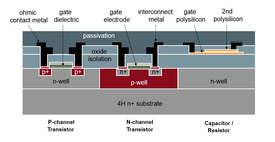
Figure 1 - Raytheon’s HiTSiC process allows for the creation of p- and n-channel transistors within a thin layer of monolithic 4H Silicon Carbide substrate. The doping profiles, dielectrics and deposited films are designed to allow 15V operation at more than 300°C.
Also worthy of note, when comparing the use of GaN and SiC for fabricating power switches, is the fundamental difference between device architectures. Currently, the inability to grow bulk GaN crystal means transistors are built laterally (flat). SiC power components on the other hand can be built vertically, so that the electrical current flows through the thickness of the substrate material. This puts GaN-based lateral devices at a disadvantage, as the heat conduction path is typically through the substrate; and if the GaN has be placed on a low-cost Si substrate, the thermal performance will be no better than that of a Si device. Also, surface breakdown can limit the voltage performance to about 600V. SiC vertical devices do not suffer in the same way, allowing for the construction of devices for use in much higher voltage applications (well into the kV region).
Components that have been fabricated in SiC include diodes, a variety of transistor types (such as MOSFETs, JFETs and IGBTs) and gate-turnoff thyristors. Hence, with access to such fundamental building blocks, it is possible to create smaller, lighter and extremely efficient power modules for switching power to/from loads and for conversion.
For instance, in May 2014, Toyota announced that, through the use of SiC power semiconductors, it aims to improve hybrid vehicle fuel efficiency by 10% (under the Japanese Ministry of Land, Infrastructure, Transport and Tourism's JC08 test cycle) and reduce automotive Power Control Unit (PCU) size by 80% compared to current PCUs with Si only power semiconductors.
SiC-based power modules also have a home in the rail sector. For example, in late 2013, Mitsubishi Electric launched a railcar traction inverter system for 1.5kVDC catenaries that incorporates what it claims to be the world’s first all-Silicon Carbide power modules; made with SiC transistors and SiC diodes. According to Mitsubishi Electric, the new traction inverter system’s switching loss is approximately 55% less than its conventional inverter system. These reductions, along with an ability to handle more regenerated energy (through regenerative braking) lead to a claimed total energy consumption reduction of about 30% compared to conventional systems. Size and weight are said to be reduced by about 65%, compared to conventional inverter systems with IGBT power modules, and about 30% compared to existing hybrid inverter systems (with SiC diodes).
Closer than before
Without doubt, Silicon Carbide is the material for high temperature and high voltage applications. However, for high speed switching applications, it is becoming necessary to locate control circuitry as close as possible to the power semiconductors; in order to minimise parasitic delays and losses. For example, under an Innovate UK supported project called LAMPS, Raytheon UK’s semiconductor business in Glenrothes, Scotland (in conjunction with UTC Aerospace Systems and others) is developing a revolutionary extreme temperature 3-phase power switch module.
![]()
Figure 2 - Raytheon’s HiTSiC project is developing an advanced SiC manufacturing technology and has demonstrated the world’s first 400°C CMOS transistors and a 300°C CMOS IC. This breakthrough process enables higher efficiency electrical energy management and advances in SiC wafer processing as well as individual device design technology.
Packaging and internal interconnect technologies are being explored which will allow the co-location of SiC switches (rated at 1.2kV/50A) with base driver circuitry fabricated using 15V HiTSiC CMOS (Figure 1) in order to maximise the module performance, and achieve a switching frequency of more than 75kHz.
Also, materials and bonding techniques are being explored with the aim of accommodating a wide temperature range and temperature cycling; as the intention is for the module to be able to work at temperatures up to 300°C. If successful, this will not only represent a significant breakthrough in PSM technology but it will also prove that previously heat-sensitive systems can be re-engineered for use in harsher environments.
SiC- and GaN-based semiconductors are starting to play a major role in a variety of sectors, where their material properties provide more efficient use of energy. Flat screen TVs, server farms and PV panels are, for example, all benefiting from lower power losses through the use of SiC-based components. However, for high voltage, high power and high temperature applications SiC is currently the only contender.
![]()
Table 1 - Silicon Carbide’s high temperature operation combined with its high voltage operation and heat transfer properties make it the most suitable material for high power semiconductors.
Avoiding traps
The mass adoption of Silicon Carbide will depend on the efficiency of, and the performance that can be delivered by, a variety of fundamental electronic building blocks; ones which are traditionally fabricated in Silicon. For instance, Raytheon UK’s semiconductor business unit in Glenrothes, Scotland, is working on a Knowledge Transfer Partnership (KTP) project, in conjunction with researchers at Newcastle University, to study the characteristics of the interface between SiC and Silicon Dioxide (SiO2), the region which critically impacts on the performance of a MOSFET.
Defects known as ‘traps’ in the interface between the two semiconductor materials affect the threshold voltage and maximum current that a MOSFET can handle. A detailed understanding of the interface behaviour will enable Raytheon UK to optimise its SiC CMOS and Power MOSFET manufacturing processes to minimise the occurrence of traps, resulting in not only higher performance devices for its own power-module devices, products and systems but also for those customers using the company’s foundry services.


