Nanowire provides 'ultimate' semi-to-superconductor contact
Researchers at the University of Copenhagen's Niels Bohr Institute are behind the discovery of a new type of ‘nanowire’ crystal that fuses semiconducting and metallic materials on the atomic scale. The breakthrough has great potential, and could lay the foundation for future semiconducting electronics, potentially enabling technologies such as quantum computation and solar cells.
The development and quality of extremely small electronic circuits are critical to how and how well future computers and other electronic devices will function. The nanowire material, comprised of both a semiconductor and metal, has a special superconducting property at very low temperatures and could play a central role in the development of future electronics.
“Our material was born as a hybrid between a semiconducting nanowire and its electronic contact. Thus we have invented a way to make a perfect transition between the nanowire and a superconductor. The superconductor in this case is aluminium. There is great potential in this,” said Thomas Sand Jespersen, Associate Professor, Center for Quantum Devices, Niels Bohr Institute, who has worked in the field for more than 10 years, ever since research into nanowire crystals began at the Institute's Nano-Science Center.
Nanowires are extremely thin nanocrystal threads used in the development of electronic components, such as transistors and solar cells. Part of the challenge of working with nanowires is creating a good transition between these nanowires and an electrical contact to the outside world. Until now, researchers from all over the world, not just at the Niels Bohr Institute, have cultured nanowires and their contacts separately. However, with the approach taken by the NBI, both the quality and the reproducibility of the contact have improved considerably.
Solids, consisting of pure atomic elements, are heated up until a desired pressure is reached in the cell. Then, a small port is opened to a vacuum chamber, where a beam of atoms from the vapour phase is directed towards a semiconductor substrate, from where the nanowire crystals are formed.
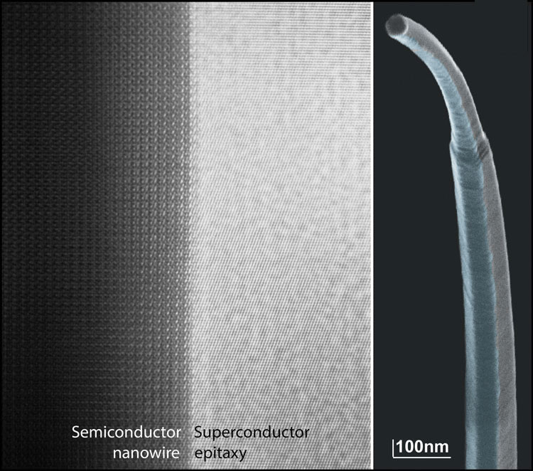
“The atoms sit in a perfectly ordered lattice in the nanowire crystal, not only in the semiconductor and the metal, but also in the transition between the two very different components, which is significant in itself,” explained Peter Krogstrup, Assistant Professor, Center for Quantum Devices, Niels Bohr Institute, who has worked hard in the laboratory to develop the contact.
“You could say that it is the ultimate limit to how perfect a transition one could imagine between a nanowire crystal and a contact. Of course this opens many opportunities to make new types of electronic components on the nanoscale and in particular, this means that we can study the electrical properties with much greater precision than before.”
In the Institute's publication in Nature Materials, the research group has demonstrated this perfect contact and its properties, and has also shown that they can make a chip with billions of identical semiconductor-metal nanowire hybrids.
“We think that this new approach could ultimately form the basis for future superconducting electronics, and that is why the research into nanowires is interesting for the largest electronics companies,” concluded Thomas Sand Jespersen.
Both Krogstrup and Jespersen are part of the Center for Quantum Devices, led by Professor Charles Marcus, and they have close research collaboration with Microsoft. The research is further supported by the Carlsberg Foundation, Lundbeck Foundation and the Danish National Research Foundation.


