Nanusens technology enables AI to be smarter
The problem at the moment is that sensors are currently manufactured on a tiny sliver of silicon, or die, by a small number of specialist companies with each sensor type being produced on a dedicated production line so it is hard to ramp up production.
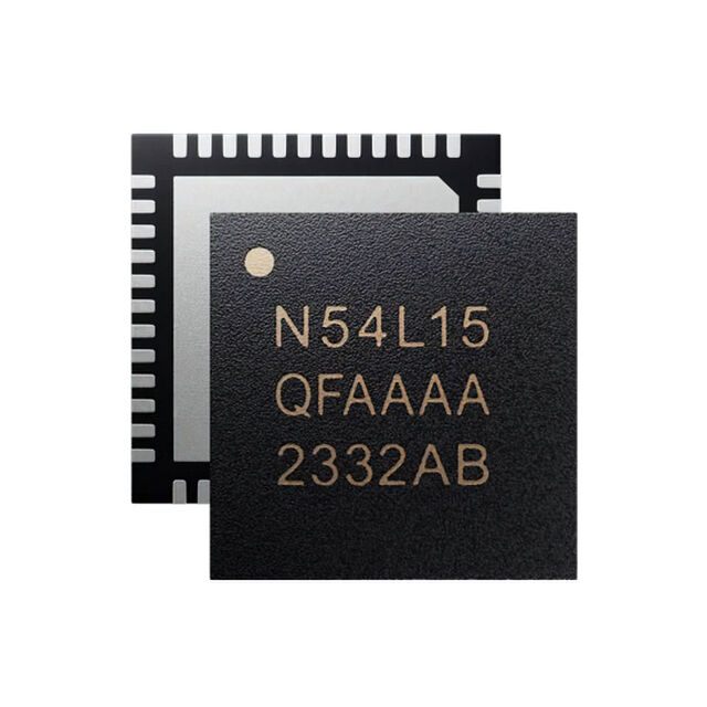
These are either packaged into the familiar black unit with wire connections to be mounted on a PCB or fixed beside the main chip as a bare die. Both approaches are relatively expensive and large with no current way to reduce costs and size forming a barrier to the advancement of AIoT.
A British pioneer of sensor technology, Nanusens, has solved these two problems. Its breakthrough is being able to create the sensors directly within the control chip of the device, or ASIC, as the chip is being manufactured. This means that the sensors only take up a virtually insignificant amount of space by being in the chip itself instead of taking up space by being packaged beside it. Also, many different sensors can be built into a chip to make much smarter devices with a negligible increase in costs or space taken up inside the device. Thus, Nanusens’ multi-sensor solution frees up space for more features and larger batteries to give a longer life in use. In addition, the power consumption is also dramatically reduced which helps extend the battery life even more.
“Being able to include as many sensors as is required within a chip for almost no size or cost penalty is going to revolutionise the design of a whole new generation of smarter AIoT devices,” explained Josep Montanyà, the CEO of Nanusens and inventor of this breakthrough. “Until now, IoT has never been able to take off as predicted because the costs of sensors were too great, the size too large, the power consumption too high and the production volumes too constrained. We are the only company to have solved not just one of these barriers but all four by at least an order of magnitude for each one. We enable masses of sensors to be deployed for almost nothing to gather the real world analogue data into the IoT network that AI needs to be effective. This is a vital role that will enable the potential of AIoT to be realised. And, naturally, we are building an extensive patent portfolio to protect our unique technology that will empower the AI and IoT revolution that is AIoT.”
Nanusens has recently proven this new technology of embedding sensors and their control circuitry with working chips that have already resulted in one license agreement and several in the pipeline. As a result, it has now started a Series A funding round.
Technology backgrounder
Nanusens have perfected the building of sensors within chips. The sensors, called MEMS or Micro Electro Mechanical Systems, are built using the standard chip manufacturing techniques, called CMOS, that are used to build the electronic circuits on chips and at the same time as the rest of the chip circuitry. This means that chips with Nanusens embedded sensors can be made in any of the many CMOS fab in virtually unlimited numbers and with the high yields that are normal in such fabs with all the benefits of low unit costs that fab production provides.
A key new innovation by the company is development of a novel control circuit that measures the capacitance changes within the sensor to provide sensor data. Like the sensor itself, this is also a digital IP block so it can be incorporated in the floor plan of the device’s control chip, or ASIC, using standard EDA tools. This pairing for sensors and control circuitry as IP is unique as no other sensor solution can be turned into an IP block and made using standard CMOS techniques within the layers of the chip structure. This also significantly reduces the complexity and bill of materials costs for an AIoT device.
Nanusens has already built accelerometer sensors into an ASIC chip using this technology. It is developing many other different types of embedded sensors such as gyroscope, magnetometer, pressure sensor, microphone, IR imagers, and gas sensor as most of these are variants on the accelerometer design. These open up many other massive markets for its embedded sensors such as smartphones, earbuds, wearables, automotive, medical equipment, and aerospace, to name but a few. As a result, the company has started a Series A funding round.


