
Analogue design: the key to feed our digital world
Milan Ivković, Director Segment Analog/Power & Technical Support Center Manager EBV Elektronik discusses how design engineers can benefit from analogue systems in tandem with the digital world.
It's easy to think that the connected world is exclusively digital. The reality, however, couldn't be further from the truth. Any application that relies on real-world environmental data, for example, to operate depends on analogue information. Temperature, humidity, air pressure, and light levels are all analogue values. Voltage, current, and radio frequency measurements are analogue too.
Many circuits operate in an analogue or mixed-signal domain – DC/DC power conversion, wireless modules, sensors, and more. Analogue signals are converted into digital representations so microcontrollers and microprocessors can efficiently process them. In doing so, the analogue signals may lose some resolution and signal fidelity as digitalisation occurs.
Some semiconductor ICs function purely in the analogue domain – examples include operational amplifiers (opamps), power conversion, and wireless transceivers.
The next sections focus on the importance of analogue design and analogue semiconductors. It will cover a few of the most frequently used analogue circuit functions, including analogue to digital conversion and sensor modules.
Life is analogue
Modern industrial automation and process control systems are responsible for bringing high levels of operational effectiveness to factories and manufacturing plants. Monitoring and control systems receive a constant stream of data from production assets, such as motors and actuators. Analogue signal acquisition and processing circuits perform vital functions in critical control loops.
Sudden or long-term data changes against predefined benchmarks alert plant management to the potential of an impending failure. Data is gathered using a variety of sensors, from simple temperature measurements to more sophisticated vibration microelectromechanical systems (MEMS).
The measurements taken are of analogue parameters, for example, the temperature in degrees centigrade (°C), vibrational in metres per second squared (m/s2), or pressure in Pascals (Pa).
Analogue to digital conversion: a function of convenience
The processing, manipulation, and interpretation of the measured data occur in the digital domain using processing devices such as microcontrollers, microprocessors, and FPGAs (field-programmable gate arrays). These devices can perform hundreds or millions of complex calculations per second, allowing other control system parts to decide if an action is required.
Getting the analogue data into the digital system takes place inside an analogue to digital converter (ADC) IC – see Figure 1.
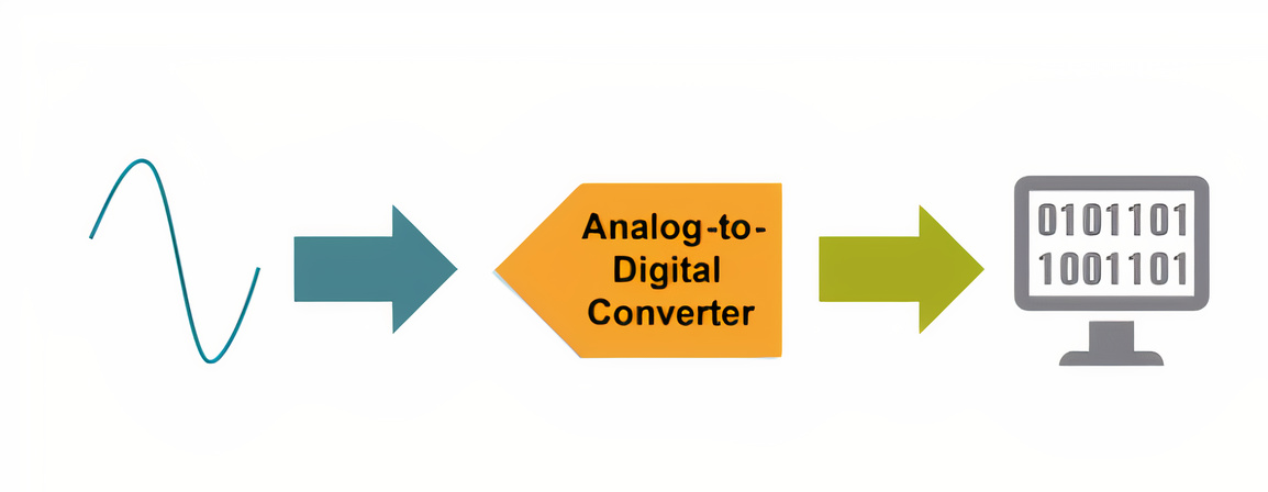
Figure 1. An analogue to digital conversion IC (source Microchip)
In simple terms, an ADC measures the analogue signal at a uniform rate and assigns a digital value to each sample. The resolution of the digital value is dependent on the number of bits used. Each digital value represents a range of analogue values, resulting in the digital output of a smooth sine wave becoming a series of digital steps or levels.
The higher the ADC's bits, the smaller the steps resulting in a high resolution. ADC ICs typically are available with 8-bit, 12-bit, 14-bit, and 16-bit resolution. An 8-bit ADC can resolve an analogue signal into a maximum of 256 levels. In contrast, a 16-bit ADC provides 65,536 levels.
Analogue applications
Sensor ICs or modules typically incorporate an ADC and a digital interface. The measurement, conversion, and connectivity functions become integrated into a single compact package with this approach, saving valuable PCB space.
Many energy-efficient microcontrollers and microprocessors also include analogue conversion features, providing development engineers with design flexibility and the opportunity to perform all conversion, processing, and interpretation functions within a single low power IC. Figure 2 illustrates a typical integrated temperature sensor IC with an integrated serial digital I2C interface.
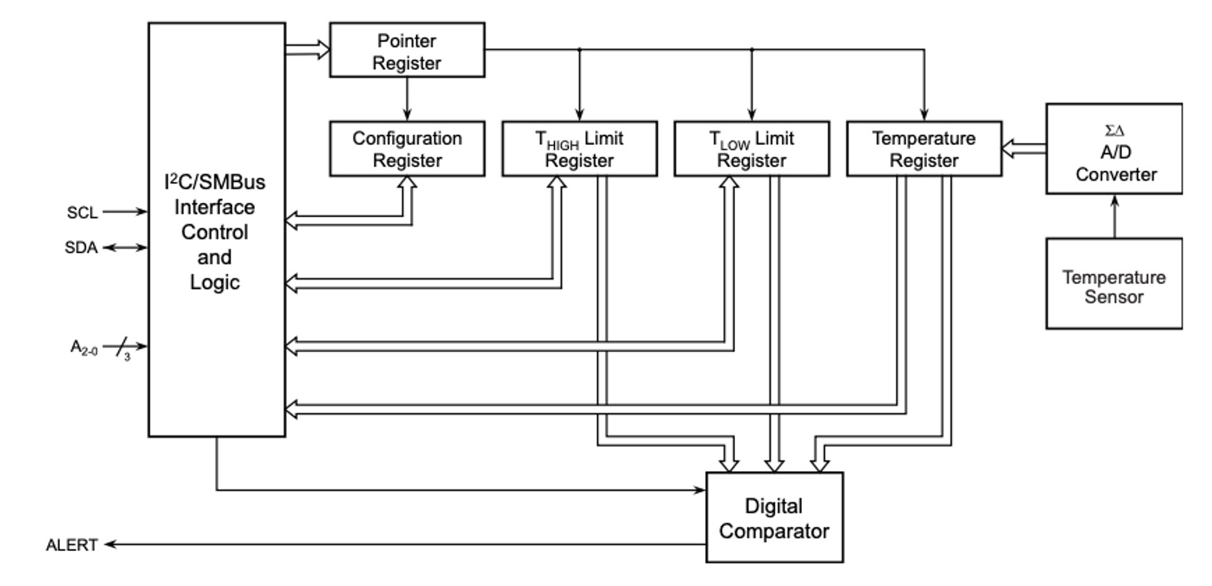
Figure 2. An example of an analogue temperature sensor IC with user-selectable ADC conversion capability and a digital interface (source Microchip)
The sensor can measure temperatures from −55°C to +125°C, and the integrated ADC is configurable from 9-bits to 12-bits. A 9-bit conversion provides a measurement resolution of 0.5°C down to 0.0625°C resolution for 12 bits.
For industrial predictive maintenance applications, such as condition monitoring, the real-time measurement and analysis of a motor's vibration profile gives a good indication of its health. Vibration is measured using a MEMS accelerometer, and the result presented in ‘g’. MEMS sensors are fabricated and finely engineered using semiconductor manufacturing techniques. Most MEMS accelerometers employ three miniature surfaces, one rigid and one able to vibrate to detect forces of acceleration or deceleration in X, Y, and Z axes (Figure 3).
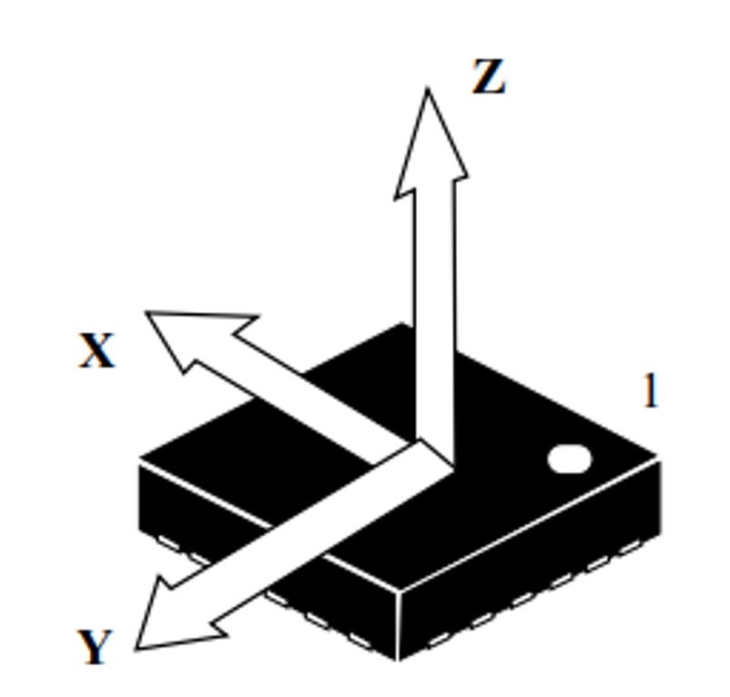
Figure 3. Measurement of acceleration and deceleration forces in three axes relative to the MEMS sensor IC package (source ST Microelectronics)
Microscopic movement of the MEMS structures results in capacitance changes between them, which, when measured, indicates the magnitude and axes of the forces present.
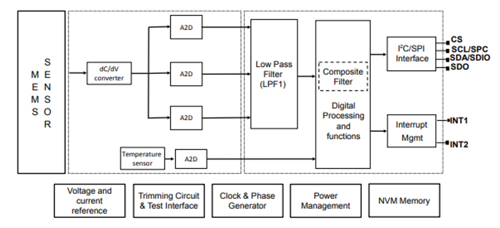
Figure 4 illustrates the construction of a typical MEMS accelerometer highlighting the major functional blocks (source ST Microelectronics)
The analogue capacitance measurements of each axis are measured and converted into digital values. After some digital signal processing techniques, the data is available for communication to the host processor via the I2C serial interface. All of the required sensor functions become integrated inside an application-specific integrated circuit (ASIC), which, together with the MEMS element, form a single system-in-package (SiP) IC.
Analogue semiconductor process technologies optimise IC power consumption profiles
Semiconductor design continues to advance. Semiconductors, such as ICs, are lithographically produced at a specific geometry that defines the size of each semiconductor process node. The smaller the geometry, the higher the transistor density, allowing more complex and sophisticated devices fabricated in a given space.
Instead of packaging a single function into a device, for example, a microcontroller, the highly integrated system-on-chip (SoC) provides the means to host a microcontroller, wireless transceiver, analogue signal processing circuitry, sensor, power management, memory, passive components, and cryptographic functions all in a single IC package. This approach is excellent news for design engineers developing space-constrained battery-powered IoT applications.
Ten years ago, a typical process node geometry was 28nm. Today 10nm and 7nm are commonplace, with semiconductor manufacturing plants, termed foundries, gearing up for 5 nm and 3 nm production. Some ICs do not require advanced process nodes, so legacy geometry ICs now represent a viable, low-cost alternative. For example, process nodes of 55m and 65nm are still in demand, particularly for semiconductors with analogue functions. Many analogue ICs still use a 300nm process.
Alongside process node developments, the process technology used to create the IC has also advanced considerably. The drivers for adopting one process technology over another, such as BCD (Bipolar CMOS DMOS), are its suitability for specific applications or electrical attributes. BCD, developed by STMicroelectronics, combines the best of both CMOS and DMOS technologies. CMOS (complementary metal oxide semiconductor) has been the stalwart of digital ICs, and DMOS (double diffused metal oxide semiconductor) is better suited for high voltage and higher power semiconductors.
Other process technologies reduce the ICs active and standby power consumption and leakage current characteristics, vital requirements for any battery-powered device, such as industrial sensors and handheld data collection devices.
Figure 5 illustrates the characteristics of the silicon on thin buried oxide (SOTB) process technology developed by Renesas compared with other technologies.
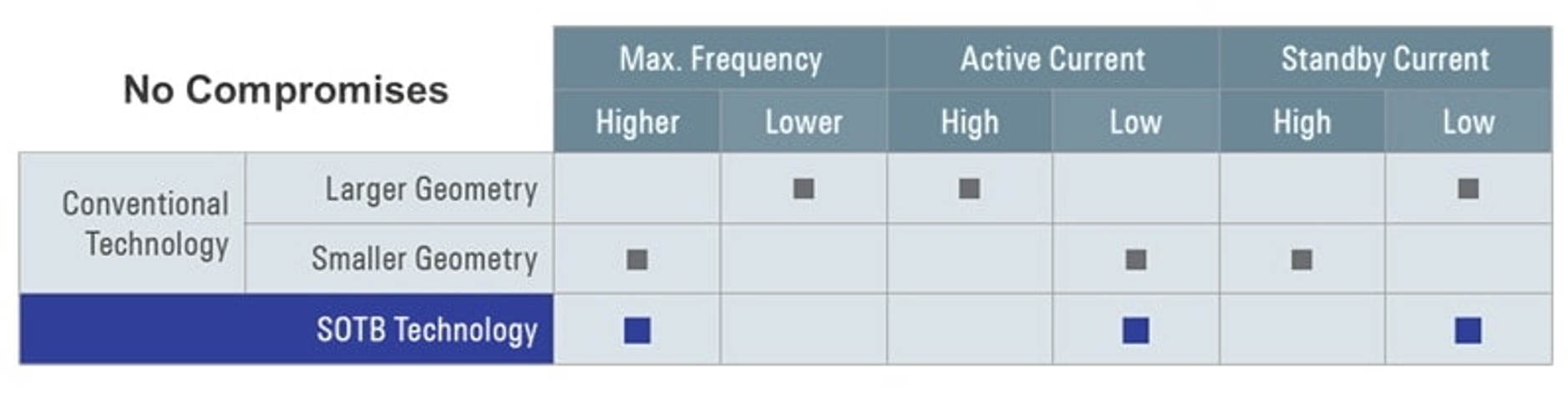
Figure 5. A comparison of the Renesas SOTB process technology (source Renesas)
Some machine learning semiconductor vendors are also turning to analogue techniques to create an extremely low power, high-density neural network IC for conducting inference at the endpoint of an industrial IoT implementation. This approach permits a dedicated neural network IC to monitor for the occurrence of specific events; for example, a motor's vibration signature suddenly changes. The rest of the monitoring circuitry can stay in the deepest low power sleep mode until the neural network IC triggers an interrupt to wake up.
Analogue simulation
Unlike many digital-based circuits, designing an analogue function typically requires more design effort and component selection. For example, using three opamps to create an active bandpass filter in a sensor's analogue front end and signal conditioning circuit. The opamp datasheet gives engineers the necessary formula to calculate the passive components, typically resistors and capacitors, to achieve the desired filter bandwidth and centre frequency.
However, working these values out for a three-stage filter involves considerable time. Another example is calculating the inductor and capacitor values for a given DC/DC power conversion module.
Analogue simulation tools significantly simplify and speed the design burden involved to complete these necessary development tasks. Online resources such as Microchip's MPLAB Mindi, ST's eDesignSuite, and Infineon's Designer provide visual and intuitive user interfaces and simulated operational results.
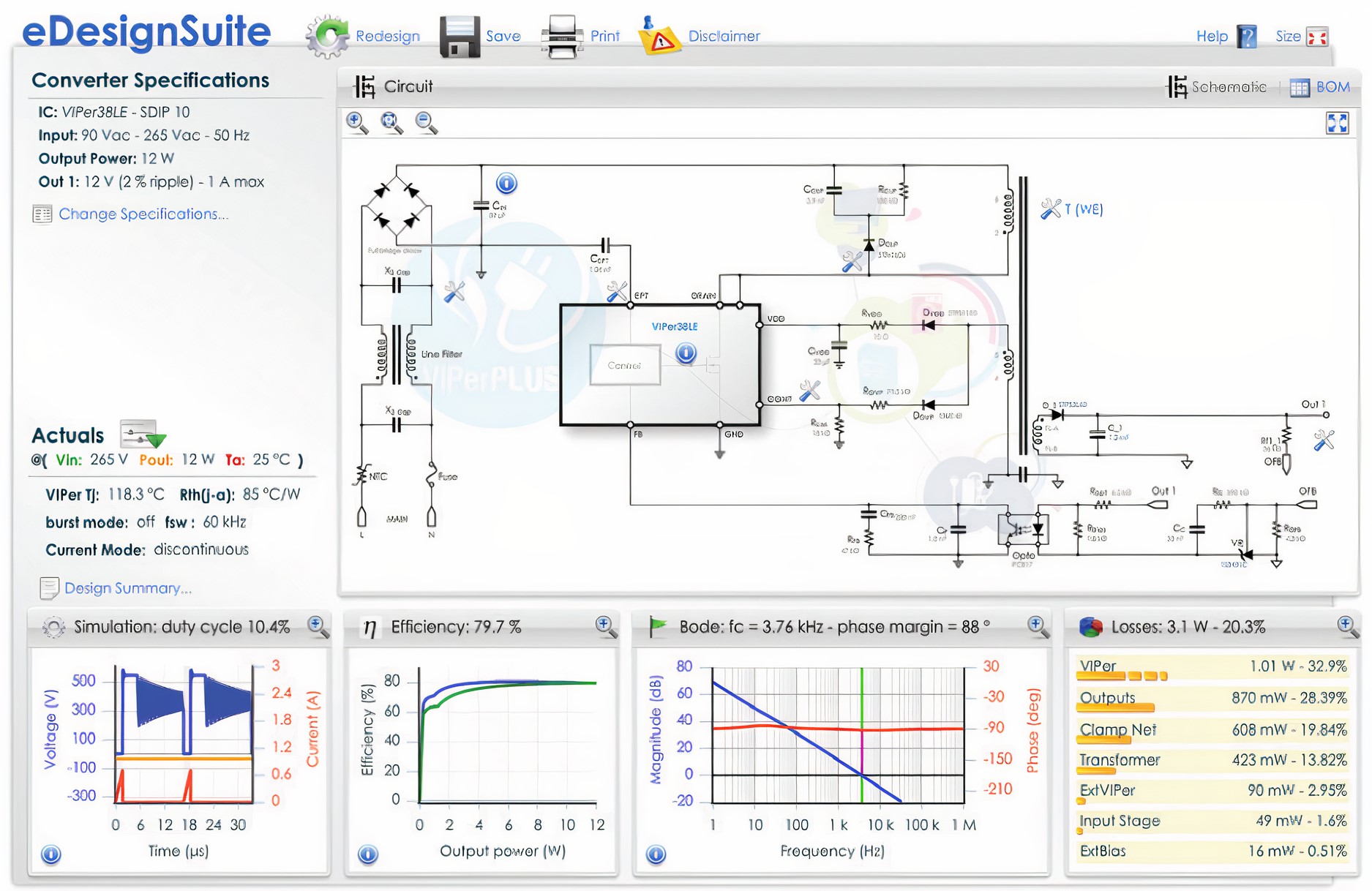
Figure 6. An example online simulation resource, the STMicroelectronics eDesignSuite (source STMicroelectronics)
Figure 6 above highlights an example of the ST eDesignSuite used to simulate the operation of a DC/DC converter across different load conditions and PWM (pulse width modulation) switching frequencies.
Analogue design: essential to our connected world
We need analogue design principles and analogue circuit functions for our analogue world. Without them, analogue devices, such as sensors, couldn't measure the temperature, or active filters wouldn't remove unwanted spurious signals.
Vendors of analogue ICs provide engineers with a host of resources such as application notes, reference designs, evaluation tools, and online circuit simulation tools that simplify the design process. Also, accessing and using analogue functions packaged within highly integrated SoCs is made easy by communicating with them over industry standard interfaces.
Put simply: for all of the above reasons and more, analogue semiconductors are a vital element of any successful design.
Product Spotlight
TBF10SL-4PS-B
ITT Interconnect Solutions

| SKU: | |
|---|---|
| Stock: | 50 |
| Cost: | $45.59 |
CAA572C0G3A663J640LJ
TDK Corporation

| SKU: | |
|---|---|
| Stock: | 1037 |
| Cost: | $9.16 |
RA1113112R
E-Switch, Inc.
| SKU: | EG5619-ND |
|---|---|
| Stock: | 5586 |
| Cost: | $0.55 |
R30-3002002
Harwin

| SKU: | |
|---|---|
| Stock: | 6545 |
| Cost: | $0.76 |
NRF54L15-QFAA-R
Nordic Semiconductor

| SKU: | 4823-NRF54L15-QFAA-RTR-ND |
|---|---|
| Stock: | 0 |
| Cost: | $2.39 |
STDRIVEG611Q
STMicroelectronics

| SKU: | 497-STDRIVEG611QTR-ND |
|---|---|
| Stock: | 0 |
| Cost: | $2.63 |
TBF10SL-4PS-B
ITT Interconnect Solutions
| SKU: | |
|---|---|
| Stock: | 50 |
| Cost: | $45.59 |
CAA572C0G3A663J640LJ
TDK Corporation
| SKU: | |
|---|---|
| Stock: | 1037 |
| Cost: | $9.16 |
RA1113112R
E-Switch, Inc.
| SKU: | EG5619-ND |
|---|---|
| Stock: | 5586 |
| Cost: | $0.55 |
R30-3002002
Harwin
| SKU: | |
|---|---|
| Stock: | 6545 |
| Cost: | $0.76 |
NRF54L15-QFAA-R
Nordic Semiconductor
| SKU: | 4823-NRF54L15-QFAA-RTR-ND |
|---|---|
| Stock: | 0 |
| Cost: | $2.39 |
STDRIVEG611Q
STMicroelectronics
| SKU: | 497-STDRIVEG611QTR-ND |
|---|---|
| Stock: | 0 |
| Cost: | $2.63 |