An valid alternative to conventional machine tooling
Gerard Young, Applications Engineering Team Leader, Parker Hannifin – Chomerics Division Europe, explains that 3D printing for prototyping EMI housings and gaskets is breaking new ground.
The introduction of affordable 3D printing services, properly known as additive manufacturing (AM) services, has allowed electronics product manufacturers to consider a new approach to the production of prototypes. A 3D printing service can in many cases form a complex, rigid structure from a CAD tool rendering much more quickly and cheaply than a traditional machine tool workshop can.
The potential for cost and time saving has sparked the interest of Parker Chomerics, which manufactures EMI gaskets and shields to customer specifications for use in end products in the aerospace, automotive, industrial and communications equipment sectors (see Figure 1). When developing the prototype of an EMI shielding solution, a casing or frame can quickly be formed by an AM machine, and then sprayed with conductive paint. When combined with a gasket dispensed on to it, an AM-based prototype can be used to prove a concept or idea. This is, potentially, much less costly and time consuming than producing conventionally machined parts.
And the more iterations of the prototype are required, the greater the accumulated time and cost savings.
For this reason, Parker Chomerics engineers are today making considerable use of 3D printing for prototyping. They have learned a number of important lessons from their experiences of using both the Parker Hannifin Corporate Technology Ventures (CTV), a new state of the art advanced manufacturing learning and development centre in Ohio, US, and commercial AM services in the product development process. Like Parker Chomerics, almost any electronics OEM could potentially benefit from the use of AM for prototyping - this article describes the considerations that must be taken into account, and the pitfalls to avoid.
Guideline 1: draw on the AM service provider’s expertise
An understanding of the AM service’s capabilities and materials is essential if the user is to produce a successful prototype. An early discussion about the design features of the CAD model and the materials available for additive manufacture is likely to be productive, helping to save time and money by reducing the number of iterations required before a successful model is made. It is particularly helpful to draw on the expertise of an AM service provider when choosing the base material and the process technology.
Two types of processes are used in industrial-grade AM - selective laser sintering (SLS) and fused deposition modelling (FDM). A third type, fused filament fabrication (FFF), is the most commonly found technology in hobbyist-grade machines, but SLS and FDM are generally the processes that produce industrial grade components. To rank the three processes in order of their cost and the complexity of the components that they can produce, at the low end is FFF, followed by FDM. At the top end is SLS.
A user’s choice of process depends primarily on the nature of the component being produced, the speed with which it needs to be produced, and the required quality of the finished item. The AM service provider can advise on this, and also on the choice of material from which the item is to be formed. Metals such as stainless steel, steel and titanium are commonly used in AM processes, as are aluminium-, copper- and nickel-based alloys.

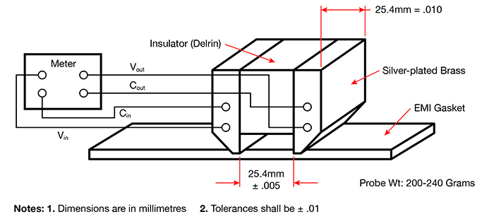
Above: Figure 1. Test set-up for continuity testing across a thickness. (Image credit: Parker Hannifin)
A range of thermoplastic compounds are also in common use today, and more are constantly being made available. Common plastics such as acrylonitrile butadiene styrene (ABS) and polycarbonate are available today, as are nylons which may be filled with glass, carbon fibres or aluminium to modify the properties of the base plastic.
The AM service’s experts will have first-hand knowledge of the performance of each of these materials after processing through an AM machine.
Guideline 2: modify the design to suit additive manufacture
Designs which are optimised for machining or moulding should sometimes be re-designed to take account of the unique nature of additive manufacture. In Parker Chomerics’ experience, it is also sometimes necessary to pay for a few iterations of the production process to achieve better accuracy than the supplier’s normal level.
This is primarily because the material is added in layers, and each layer has a minimum thickness. It is often advisable to design the part’s nominal dimension to match the thickness of an integer number of layers.
The user’s choice of AM material might also have to find a balance between the need to produce adequate mechanical properties for the needs of the application while also matching the properties of the material from which the production component will eventually be made. For instance, in order to achieve a certain stiffness and elastic modulus in the AM part, the user might have to accept that its thermal performance deviates somewhat from that of the production component.
A careful choice of prototyping substrate will ensure that its mechanical and thermal properties are sufficiently close to that of the machined metal or conductive polymer from which a production component will generally be made.
Guideline 3: match the paint to the AM material
The AM process produces a formed part with the specified mechanical properties – but if it is to have useful EMI shielding properties, it needs to be sprayed with a conductive coating. Suitable acrylic or epoxy paints include the Cho-shield 2056 or Cho-Shield 610 products from Parker Chomerics, which include conductive fillers. These coatings have a known thickness which needs to be taken into account when designing the part.
Conductive coatings such as the products from Parker Chomerics are optimised for application to standard materials such as metal or thermoplastics. The interaction between AM materials and conductive coatings can be different.
To ensure a good result it is preferable to first spray a test piece to ensure that the paint system does not adversely affect the part. These coatings often contain solvents which can damage the part, or which need to react with the surface in order to adhere to it.
Normally, one-part acrylic paints are sprayed onto surfaces such as polycarbonate or ABS, and the solvents in them result in good paint adhesion. Two-part epoxies are used on metals and other substrates that do not react with the chemicals in the coating. The choice of one- or two-part coatings will depend on the type of AM material used.
It is also very important at this stage to ensure that the painting is done by an experienced operator. It is easy for an operator with no experience with conductive coatings to produce a poor finish, because they behave so differently to normal decorative or protective coatings.
Guideline 4: some am materials do not support accelerated curing
After spraying the part, the coating must be cured. Here again, careful consideration must be taken of the difference between the chosen AM material and the material from which the production part will be made. Some AM materials will not tolerate oven curing at all: curing at room temperature might take up to a week, and this detracts somewhat from the speed advantage that prototyping with AM processes normally affords.

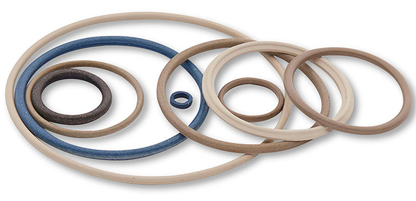
Above: D-ring and O-ring gaskets from Parker Chomerics offer EMI shielding and provide a moisture/pressure seal. (Image credit: Parker Hannifin)
Even if the AM material can tolerate oven curing, users should establish the highest temperature that can be used without damaging its structure, and accept a longer curing time when baking at lower temperatures.
Guideline 5: test the part’s electrical performance carefully
Once the paint is cured, the user needs to check the conductivity and continuity of the conductive surface. This generally requires the use of a four-point low ohmmeter in conjunction with an appropriately designed probe, such as the Parker Chomerics Cho-probe. Continuity may also be measured across a thickness with two parallel plates (see Figure 1).
Once the resistivity has been checked and approved, the next stage is to apply the gasket. Depending on the geometry of the prototype, this could be as simple as an O-ring made from conductive elastomer such as Cho-seal (see Figure 2). More complex assemblies might require the attachment of an A-section to a tang formed on the part, or dispensing form-in-place gasketing such as Cho-Form.
If using form-in-place gasketing, the same considerations apply with regards to curing as were listed for conductive coatings above.
Guideline 6: test the final assembly
Once the gasket is applied and, if necessary, cured, the final stage prior to inserting the item in the host device is to apply a final resistivity check. The resistivity check can be performed by applying probes to the gasket in certain positions and loadings around the component. It could alternatively be tested in a fixture that simulates the final assembly and use. In either case, care should be taken not to over-compress the gasket or to damage the coating or component.

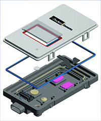
Above: Integrated solution by Parker Chomerics incorporating EMI shielding and thermal materials. (Image credit: Parker Hannifin)
Speed and cost advantages
What the Parker Chomerics engineers who design custom EMI shielding solutions have found is that AM provides them with a new way to prototype a design more quickly and more cheaply than by conventional methods. Care must be taken, however, to ensure the right process is chosen and the correct material selected. It always pays to take advice from the AM service provider on this, and to use its recommendations to modify the design to make it suitable for additive manufacturing.


