Top five power products in May
Here, Electronic Specifier takes a look at the top five power products released in May.
1) EPC has announced the availability of the EPC9149, a 1kW-capable 48V input to 12V output LLC power conversion demo board that operates as a DC transformer with a conversion ratio of 4:1. This demonstration board features the 100V EPC2218 and 40V EPC2024 GaN FETs.
The board is the size of DOSA-standard ⅛th brick format, measuring only 58.4x22.9mm. This is considerably smaller than alternative silicon-based solutions that are generally sized in the ¼th brick format, or twice as large, for 1kW of output power.
The total thickness of the converter without heatsink is only 10mm. To make it simple for a power supply designer to easily replicate this design, all supporting materials for this board including schematic, bills of materials, and Gerber files are available on the EPC website.
The high-power density, 1,226W/in3, is achieved thanks to EPC GaN FET technology. eGaN FETs enable high switching frequency, in this case 1MHz, and they are very small, ⅓ of the size of silicon MOSFETs with similar on resistance.
The EPC9149 board features four 100V rated EPC2218 eGaN FETs for the primary rectification, and eight 40V rated EPC2024 eGaN FETs for the secondary synchronous rectification. The board also features a 4x4mm Microchip dsPIC33CKMP102T-I/M6 for flexibility, configuration, communications, and programmability.
This new demonstration board can operate from an input voltage between 36 and 60V and delivers up to 83.3A load current. The peak efficiency from 48 to 12V is 98% and the full load efficiency, at 12V when delivering 1kW, is 97%. The highest temperature in steady state operation at maximum load with 400 LFM airflow is 88°C, which relates to a maximum junction temperature of 95°C.
2) Nexperia has announced new 0.55mΩ RDS(on) 40V power MOSFETs in the high-reliability LFPAK88 package for automotive (BUK7S0R5-40H) and industrial (PSMNR55-40SSH) applications. These devices are the lowest RDS(on) 40V parts that Nexperia has ever produced and more importantly, they deliver greater power densities than traditional D2PAK devices.
The new devices also offer improved performance in both Avalanche and Linear mode, leading to increased ruggedness and reliability.
Neil Massey, Nexperia’s Product Marketing Manager commented: “The new 8 x 8 mm LFPAK88 MOSFETs combine the latest high performance superjunction silicon technology with our proven LFPAK copper clip technology, which is renowned for delivering significant electrical and thermal performance benefits. The resulting low RDS(on) enables us to pack more silicon in the package, improving power density and shrinking device footprint.”
Measuring just 8x8x1.7mm, the new power MOSFETs also feature class-leading linear mode / safe operating area (SOA) characteristics for safe and reliable switching at high current conditions. SOA at 1ms, 20 VDS operating conditions is 35A due to a combination of silicon and package, while at 10ms, 20 VDS where the package dominates, SOA is 17A. The devices also offer the best single pulse avalanche rating (EAS) at 2.3 J and very strong ID current rating of 500A, which – unlike some competing devices – is a measured rather than theoretical limit.
The size and performance benefits afforded by the Nexperia 8x8mm LFPAK88 MOSFETs enable designers to replace two paralleled old-style components with one new LFPAK88, simplifying manufacturing and increasing reliability.
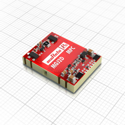
3) Murata has added to its expansive range of advanced power solutions, with a new series of surface mount DC/DC converters. Comprising nine different models, the lightweight units in the MGJ2 series each have a two watt power rating and are supplied in compact, low-profile form factor modules with 19.49x14.99x4.39mm dimensions.
They are intended to accompany the IGBT and SiC-based MOSFET high-voltage gate drivers used in industrial, renewable energy and mobility applications. Available in input versions that accommodate the commonly-used five volt (in development), 12 and 15V voltage rails, they feature +15V/-5V, +15V/-9V and +20V/-5V bipolar outputs.
The new MGJ2 DC-DC converters exhibit an ultra-low isolation capacitance of just 3pF (typical). This helps them to mitigate the coupling of transients across the isolation barrier and prevent EMI issues from occurring due to circulating currents generated by high frequency signals.
Their characterised partial discharge performance means that elevated levels of operation can be maintained despite the demanding nature of the high-voltage applications they will be used in. Likewise, the common-mode transient immunity (CMTI), which exceeds 200 kV/µs, allows them to deal with high switching frequencies.
Other key attributes of the MGJ2 units include a continuous barrier that withstands voltage that reaches 2.5kV (also tested to cope with 5.7k VDC for a one minute period), plus 9mm creepage and clearance separation distances.
An extended operational temperature range of -40 to +100˚C is supported, and they have built-in short circuit protection mechanisms too. UL62368 compliance (for 250 VAC reinforced insulation) has already been secured, with ANSI/AAMI ES60601-1 certification currently pending.
4) Transphorm and Silanna Semiconductor has announced GaN power adapter reference design. The solution is an open frame, 65W USB-C Power Delivery (PD) charger that combines Transphorm’s SuperGaN Gen IV platform with Silanna Semiconductor’s proprietary Active Clamp Flyback (ACF) PWM controller. Together, the technologies yield an unprecedented peak efficiency of 94.5% with an uncased power density of 30W/in3.
These performance levels outpace the currently available competing solutions using silicon superjunction MOSFETs or e-mode GaN transistors, and furthermore utilise a smaller GaN FET from Transphorm. Silanna Semiconductor and Transphorm’s universal GaN adapter design is ideal for powering laptops, tablets, smartphones and other IoT devices.
The new reference design relies on advanced technologies from both Transphorm and Silanna Semiconductor. The SuperGaN FET is Transphorm’s TP65H300G4LSG, a 650V 240mΩ device in an industry standard PQFN88 package. It leverages the SuperGaN Gen IV platform, which uses advanced epi and patented design technologies to improve performance. The robust GaN FET also offers the high reliability synonymous with Transphorm devices, including the industry’s best gate robustness.
5) STMicroelectronics has announced a new family of ST Intelligent and Integrated Gallium Nitride (GaN) solutions, STi2GaN. STi2GaN is an innovative offering combining power and intelligence in compact, high-performance solutions required by the automotive industry as it shifts to electrified platforms.
Building on ST’s leadership and strong automotive experience, innovations in Smart Power technology, wide bandgap semiconductor materials and packaging expertise, the STi2GaN family combines a monolithic power stage along with drivers and protections in GaN technology as well as System-in-Package (SiP) solutions for application-specific ICs with additional processing and control circuitry. The STi2GaN solutions use ST’s novel bond-wire-free packaging technology to provide high robustness, reliability, and performance.
“STi2GaN continues ST’s long success story in compound materials and Smart Power product innovation, targeting mainly automotive applications and the needs of high-density, high-reliability and high-power. Initial offering of STi2GaN solutions suit On-Board Chargers, LiDAR for autonomous driving, bidirectional DC-DC converters, Class-D amplifiers and power conversion systems,” said Alfio Russo, Group VP and GM Low Voltage and STI2GaN Solutions Macro Division, STMicroelectronics.
“The new product family aims to leverage the high-power density and efficiency of GaN to offer an industry-unique range of devices in 100V and 650V clusters that ensure scalability, compactness, and outstanding performance.”


