Nano-pulse is a driver for DC/DC design
An automotive primary buck DC/DC converter uses a patented technology, reveals David James, Rohm Semiconductor
Traditionally the car battery was a lead-acid type with a maximum voltage of 42V. Newer vehicles, especially hybrids, are using lithium-ion batteries where voltages can be up to 60V. This has advantages for efficiency and reliability of the vehicle electronics, but it creates a serious problem for existing buck converters. High voltages are also used in industrial applications where they may be supplied directly from AC/DC converters. Most of the sub-systems or modules require supplies of 5.5V or less, typically 3.3 or 2.5V to supply a CPU. From theory in a buck converter, the maximum ratio of Vout / Vin is determined by the minimum on time and switching frequency (fSW).
For a fixed switching frequency, the buck converter must control Vout by changing the TON. Alternatively the buck converter could control Vout by changing the switching frequency but this can cause EMI issues.

Rohm has developed the BD9V100MUF-C synchronous buck primary DC/DC converter for automotive applications, based on its proprietary Nano-pulse technology. It is capable of output voltage of 5.5V or less (set be external resistive network for flexibility) with a maximum IOUT of 1A and an accuracy of ±2%. The typical Vin can be 60V, but the device will tolerate up to 70V.
Nano-pulse technology
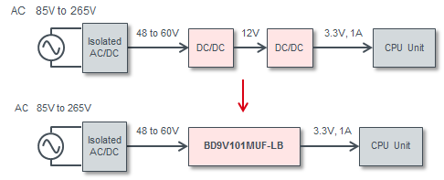
In automotive applications, the switching frequency should be lower than 600kHz, or at least 2MHz, to avoid creating interference in the AM radio band. A higher frequency would reduce the size of the external components but it also reduces the efficiency of the converter. Unfortunately the current generation of buck converters have a minimum Ton of 30ns, which means that they cannot generate 2.5 or 3.3V (typically required by most sub-systems) directly from a 60V at this frequency. In this case, both a primary and a secondary DC/DC would be required, increasing the system costs. Figure 1 illustrates the two options.
Using Nano-pulse IP, the BD9V100MUF-C is claimed to achieve a best-in-class minimum Ton of 9ns and achieves a voltage conversion from 60V to 2.5V or less in a single stage. Although the technology’s details are confidential, the company will say that it involves monitoring the switching current and careful noise rejection techniques and results in cost and PCB area reductions.
Safety functions
Safety function protect the device against external faults, and ensure safe operation in any application.
The under voltage lockout (UVLO) circuit will stop the converter switching if Vin is too low for safe operation. To reduce current consumption during operation without any load (Iq) there is an enable pin. After activating this pin, or when the VIN has become high, the device always re-starts using a soft start.
The short circuit protection protects against temporary external faults such as a short to ground on the load. If the on time is longer than expected the converter will stop switching (output will be high impedance) and then restart.
The over current protection circuit detects the lower limit of the inductor current. The integrated high side MOSFET will not turn on until the current falls below the limit. If OCP is detected multiple times, the device will stop switching for approximately 30ms before re-starting
The over voltage lockout (OVLO) disables the device if Vin is too high, and recovers when Vin falls. When the voltage falls it will restart with a soft start. When the feedback voltage reaches the target, the power good open drain output is set to high impedance. If feedback voltage is out of range, the voltage is pulled low. This output can be used as a reset signal for other devices with an external pull up (RPGD). Another safety feature is over voltage protection which will turn off the output MOSFETs if the feedback voltage is too high. When the voltage falls it will restart with a soft start. Finally, when the junction temperature is too high, the thermal shutdown circuit will disable the MOSFETS. It will recover automatically when the junction temperature falls.
Application example
Intended to reduce PCB area and minimise BoM, the BD9V100MUF-C is illustrated in an application in Figure 2. The input and output voltages are buffered by two capacitors (CIN and COUT). The output voltage is set by the external resistive network (RFB1 and RFB2) for flexibility. The switching frequency is temperature independent and set by an external resistor (RRT) for accuracy and there is an external compensation network (RCOMP and CCOMP) to optimise the frequency response. The internal regulation requires a decoupling capacitor (CVREGH) and a boot strap capacitor (CBST). The bootstrap resistor (RBST) is used to reduce EMI and the pin VMON is protected from the inductive load by a resistor (RVOUT).
Figure 2: Application schematic of the BD9V100MUF-C


