More power, less heat
Advances in MOSFET silicon and package technologies are critical to improving energy efficiency and reducing the heat generated during power conversion, says Georges Tchouangue, Toshiba Electronics Europe.
Today’s smartphone-carrying, environmentally-aware consumers understand that hot enclosures or power adapters mean wasted energy that shortens battery life and increases CO2 emissions. When making decisions about small consumer devices, home appliances, industrial machinery, or highly electrified conventional or hybrid cars, these knowledgeable buyers equate better energy efficiency with superior performance, lower ownership costs, and reduced environmental footprint.
Efficient power conversion
Historically, improvements in conduction performance have been achieved at the expense of poorer switching characteristics, and vice versa. The latest trench technologies have broken this trade-off, and enable better conduction and switching performance to be achieved at the same time.
As far as device technology is concerned, trench MOSFETs have evolved through several generations, each benefiting from advances such as improved trench pitches. This enables trenches to be more closely spaced, resulting in lower on resistance per die area. At the same time, device capacitances can be kept low, which is essential to improve switching performance and minimise the load placed on gate-driver circuitry. Toshiba’s UMOS IX-H MOSFETs improve key figures of merit such as RDS (ON) x A (on resistance x area) and RDS(ON) x Ciss (on resistance x input capacitance), resulting in better conduction performance and lower gate-drive losses. In addition, reduced output capacitance (COSS) reduces output charge (QOSS) leading to better switching efficiency.
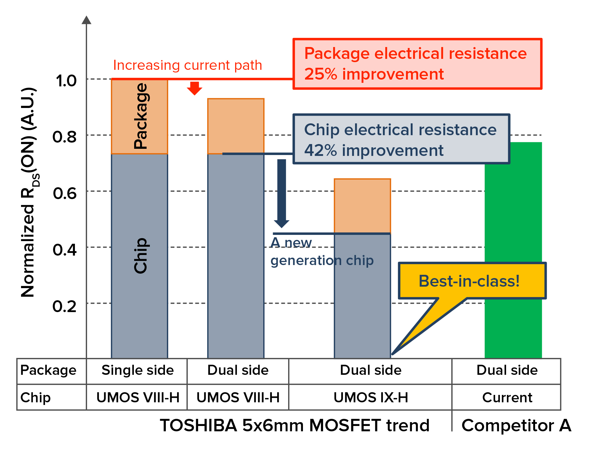
The improvements in the UMOS IX-H silicon, compared to the UMOS VIII generation, have helped realise a 42% saving in die resistance, says Toshiba, which has launched 30 and 60V N-channel MOSFETs. The 30V devices have ultra-low RDS (ON) of 0.6mΩ (max.) at VGS = 10V, and 2160pF typical COSS. For the 60V MOSFET, RDS (ON) is 1.3mΩ and typical COSS is 960pF.
Package technology steps up
Improvements at the silicon level alone are not enough to deliver the advances demanded by today’s markets. More advanced packages are also needed, to not only minimise electrical resistances but also ensure low junction-to-ambient thermal resistance allowing the device to support higher operating current. This in turn helps minimise overall component count and increase power density, thereby enabling designers to create smaller, slimmer end products without compromising overall reliability.
Key package developments seek to improve cooling and eliminate known weaknesses in traditional power packages, such as the wire bond connections between the die and the leadframe. These wire bonds limit current-carrying capability and are also vulnerable to failure.
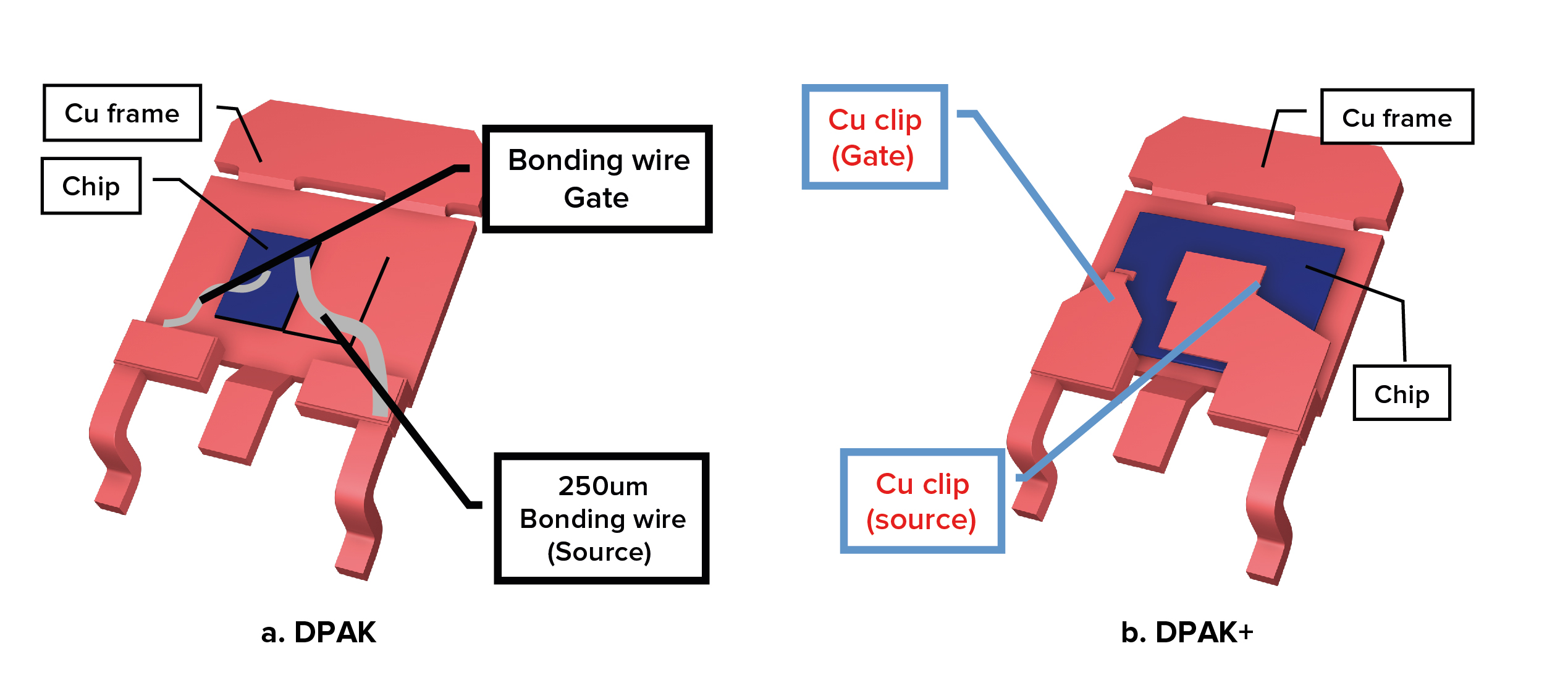
A new DPAK+ power package has the same dimensions and outline as the conventional DPAK but uses copper clips to connect the gate and source pins directly to the metallised electrodes on the die. These copper clips replace the aluminium bond wires, and benefit from a large cross-section and increased contact area at the die. This has yielded a strong improvement in package electrical resistance, reducing the contact resistance tremendously. This significantly reduces I2R losses, and also allows higher maximum current. In addition, thermal efficiency and overall reliability are improved. Figure 1 compares the more efficient and robust copper-clip gate and source connections with traditional wire bonds.

Figure 1: Bond wires versus copper-clip gate and source connections
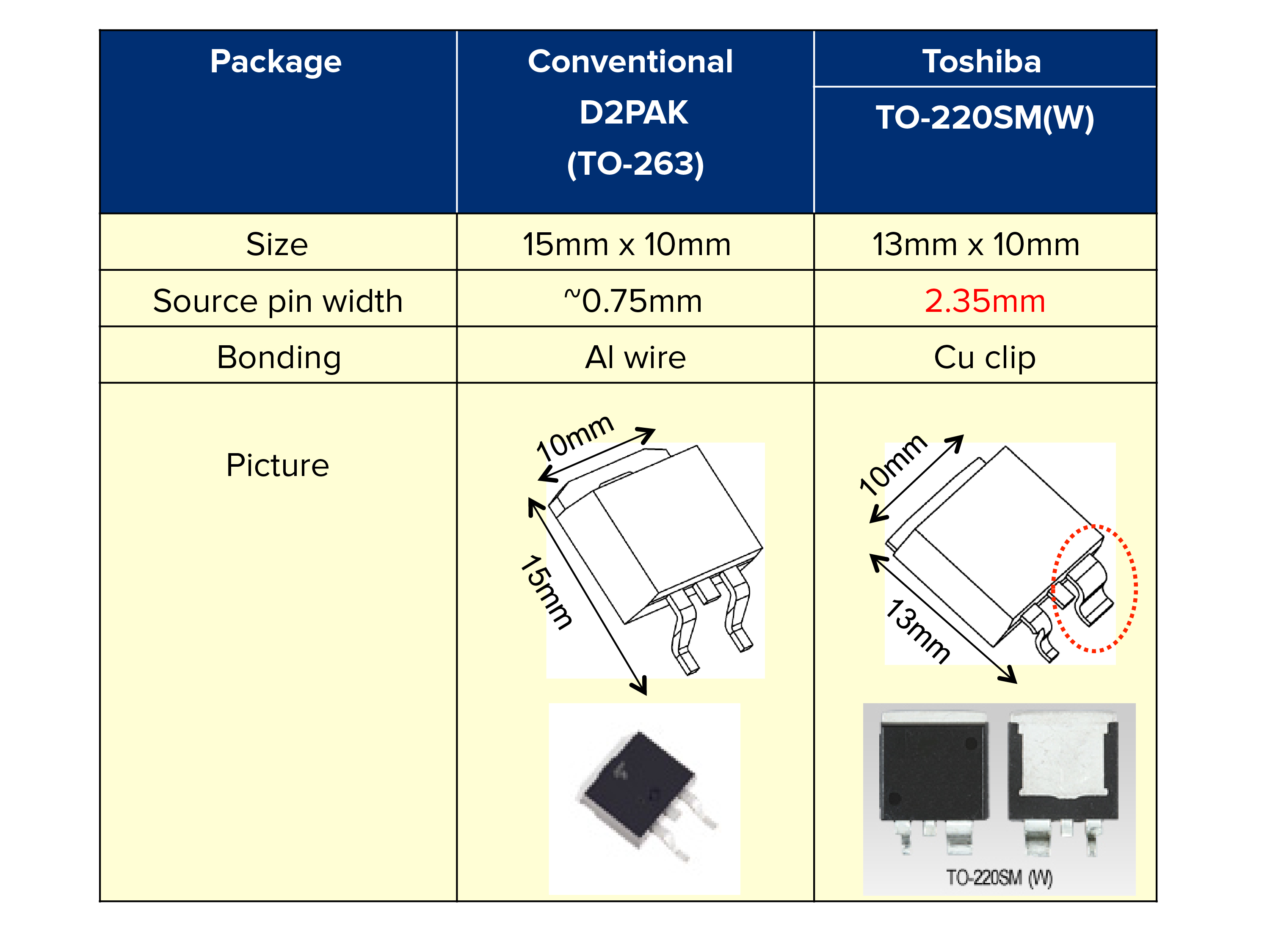
The TO-220SM(W) power package, which also features copper-clip technology, has an outline comparable to that of the conventional D2PAK (TO-263), but in addition has a source pin more than three times wider. These enhancements boost maximum current rating to 200A, while reducing the total board footprint by more than 13% to just 13 x 10mm.
Dual-side dissipation
A further new package technology, DSOP Advance, greatly improves thermal performance within space-efficient dimensions by exploiting both the top-side and underside for heat dissipation.

Figure 2: Conventional D2PAK (TO-263) vs Toshiba TO-220SM(W)
The company has introduced its first UMOS IX-H power MOSFETs in DSOP Advance. It has the same footprint as 5 x 6mm SOP. Internally, the source metallisation on the upper surface of the die is connected directly to a large electrode on the top side of the package. This not only utilises the upper package surface to dissipate heat, but allows the drain electrode on the underside to be much larger than is possible in the conventional SOP. DSOP devices can be used with an ordinary FR4 substrate and can help to significantly reduce system temperatures, giving designers extra freedom to specify smaller heatsinks.
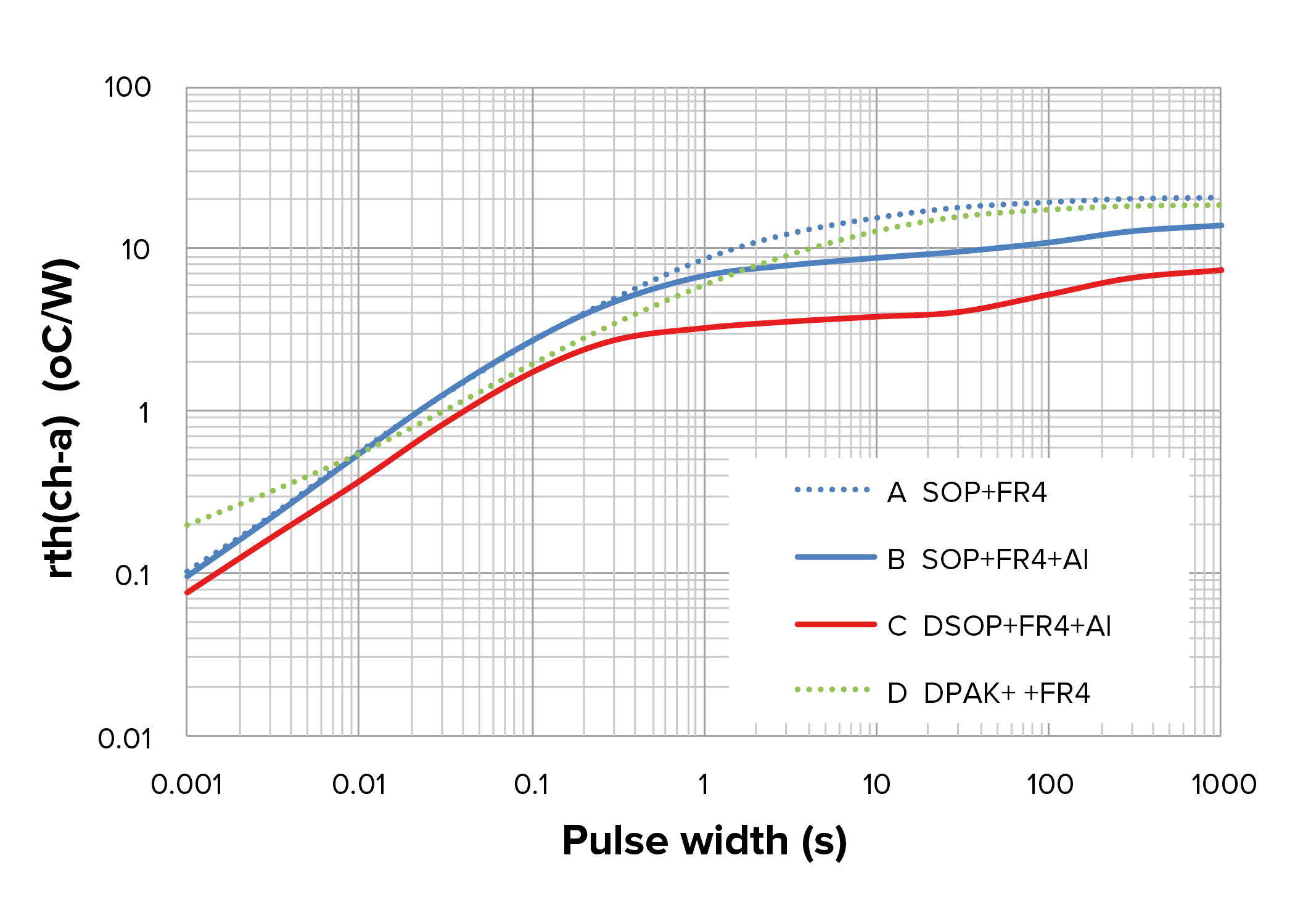
Testing the DSOP Advance alongside the conventional SOP has shown a 26% improvement in dynamic thermal resistance (RTH). Figure 3 compares the dynamic RTH of both packages when test currents of varying pulse widths are passed through the device.

Figure 3: DSOP Advance significantly improves dynamic thermal resistance
Figure 4 compares the cross section of DSOP Advance with conventional SOP and a competing dual-side package. The construction of the competing package is closely related to the conventional SOP, and uses a stacked connector to expose the pad on the upper surface. This type of construction introduces inter-facial thermal resistances between the elements of the stack, as shown, whereas the DSOP Advance with its one-piece integrated connector achieves greater thermal efficiency.

Figure 4: Comparison of single-side and dual-side cooled packages
Examining the combined effects of UMOS IX-H MOSFET technology and DSOP Advance reveals an improvement of more than 35% in device RDS (ON), as figure 5 illustrates.

Figure 5: Best-in-class efficiency of the latest-generation UMOS IX-H MOSFETs in DSOP Advance
Integration levels
Other thermally enhanced packages such as SOP Advance, TSON Advance and PS-8 maximise heat dissipation through the under-side of the device only, and are suited to cost-sensitive applications at lower power levels. TSON Advance achieves comparable power dissipation to the conventional 5 x 6mm SOP-8, yet at 3.3 x 3.3mm its footprint is 64% smaller.
The 2.8 x 2.9mm PS-8 8pin flat-lead package is suitable for small motor drives and solenoid controllers, which are commonly used in automotive systems, and has a profile of only 0.8mm. Toshiba has used this package to create the TPD7104F integrated gate driver for high-current MOSFETs such as the new UMOS IX-H family. The driver integrates all the necessary logic-control and protection circuitry, as well as a charge pump to generate the gate voltage needed for high-side gate control in PWM applications.
To help accelerate the development of motor-control applications utilising the latest MOSFETs and drivers, a number of reference boards are available that implement various control schemes such as sinusoidal commutation, low-side PWM or H-bridge driver.
Power electronics designers face constant pressure to achieve energy efficiency within smaller PCB sizes and lower overall height, while also managing heat effectively using the minimum of expensive additional parts, such as heatsinks. The latest Trench MOSFET technology significantly enhances efficiency thereby lowering heat generation. New package technologies such as Copper Clip and DSOP Advance featuring top-side and underside exposed thermal pads also help enhance and simplify thermal management to meet a variety of applications across a variety of markets and environments.


