GaN devices for power electronics are verging on big growth
GaN devices for power electronics are on the verge of big growth, but what are the driving forces behind this growth? Sally Ward-Foxton investigates for ES Design magazine.
There’s no doubt about the potential GaN technology has to make money, but just how much money, and when it will start to happen, are still under debate. A comprehensive report on the market for GaN power devices by analyst firm Yole Développement predicts big growth for the sector in the next five years: “Overall, 2020 could see an estimated device market size of almost $600m, leading to approximately 580,000 6" wafers to be processed,” explains Yole’s Dr Philippe Roussel. “Ramp-up will be quite impressive starting in 2016, at an estimated 80% CAGR through 2020.”
What’s also interesting is that the report forecasts GaN to generate just $10-12m in device sales this year. Clearly, this market is on the verge of major growth, but hasn’t yet reached tipping point. Some recent mergers and acquisitions, along with license agreements, certainly point to companies preparing for growth in the sector. For example, power GaN device company, Transphorm, recently made a deal with Fujitsu whereby Fujitsu’s GaN division will become a wholly owned subsidiary of Transphorm. In exchange, Fujitsu got a minority equity position in Transphorm. Transphorm also bought an exclusive license for Furukawa’s GaN IP portfolio. These types of deal can signify that the industry is maturing.
The reason GaN devices are so appealing is that they offer performance benefits compared to their silicon equivalents. GaN has a higher critical electric field strength than silicon, allowing a device with a given on-resistance and breakdown voltage to be made smaller in GaN than silicon. To put this another way, comparable sized devices can offer much higher breakdown voltages, useful in the field of high-voltage power conversion. The trouble is that manufacturing GaN power transistors requires growing GaN on a substrate, such as Sapphire, known to command a high price premium. The most cost effective substrate is silicon, but there is a big mismatch with the lattice spacing of the two materials; multiple layers of material is essential to reduce the physical strain on the materials and reduce the thermal differential.
Driving the growth
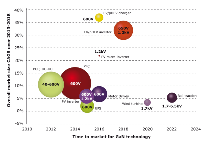
So, where is this massive predicted growth going to come from? Power supplies and PFC (power factor correction) applications will dominate until 2018, representing 50% of GaN device sales in this time frame, say Yole (see Figure 1). Specifically, GaN is particularly suited to UPS (uninterruptible power supplies). “In UPS applications, the medium-power segment is likely to be very much in line with the GaN value proposition, and savings at system level will be demonstrated,” reveals Dr Roussel. “We think GaN technology could grab up to 15% of market share in this field by 2020.”
Figure 1 - The estimated accessible markets, growth rate and time-to-market for the main GaN applications (Source: Power GaN Market, Yole Developpement, June 2014)
One rapidly growing segment within power conversion that holds potential for GaN is photovoltaic inverters. Unfortunately, while GaN devices offer benefits to PV inverters, the industry has already largely adopted competing technology Silicon Carbide (SiC), meaning it could be harder for GaN to enter this market now that there is an incumbent technology to be displaced. GaN’s advantage could lie in its cost efficiency, though. According to a 2013 report from Lux Research (‘Reaching for the High Fruit: Finding Room for SiC and GaN in the Solar Inverter Market’), GaN-on-silicon offers the lowest cost solution, with GaN-on-Sic and SiC-on-SiC offering superior efficiency.
Motor drives represent a smaller than expected market in Figure 1, partly because being a mature market, this sector is already very cost-sensitive. GaN isn’t expected to achieve price parity with silicon until 2018, so the market by 2020 is only $45m, according to Yole’s figures.
Electric and hybrid electric vehicles are another sector driving demand for high-voltage power electronics, including GaN devices. Yole predicts this application will become significant for GaN by 2018. With the cycle for automotive qualification taking up to five years, 2018 is the approximate date that EVs designed today will hit the market. This time lag also means that since GaN manufacturing technology will hopefully have matured in this time, GaN devices will have a cost comparable to that of silicon, but with better performance (faster switching and better high temperature characteristics).
Looking further into the future, for 2020 and beyond, Yole has earmarked forms of renewable energy such as wind turbines, and sectors with very long lead times such as the railway traction market, as key growth areas for GaN devices.
Preparing the technology
Coming back to the short-term, companies are continuing to innovate, developing and refining GaN technology in readiness for this predicted boom. At the APAC show this spring, Transphorm announced new reliability data for its GaN devices. The company has been carrying out extended lifetime tests, in which they accelerate lifetime testing using high voltages (1100-1150V). The results predict greater than 100m hours of lifetime when running the transistors at 480V, or 10 million hours when run at 600V. Of course, there is still no data from failures in real-world applications, but that will follow in due course. Transphorm is also testing its devices by putting them under thermal stress and continuing to test devices every lot for lifetime on an ongoing basis.
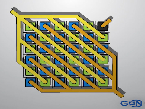
Fast forward to PCIM Europe in May, and GaN Systems announced two new series of GaN transistors for different applications, based on the company’s ‘Island technology’ (Figure 2). Rather than the finger-shapes found in a traditional transistor, each device is on its own separate island, with the gate around it. This not only reduces space, it means more current can be handled. Both the new product series come in the company’s near chipscale, embedded GaNPX package which eliminates wire bonds, thereby minimising inductance. It also optimises thermal performance and is extremely compact.

Figure 2 - GaN Systems’ island technology. Rather than the finger-shapes found in a traditional transistor, each device is on its own separate island, with the gate around it
The first, a series of five normally-off 650V GaN transistors, is optimised for high speed system design. The GS66502P, GS66504P, GS66506P and GS66508P are respectively 8.5A/165mΩ, 17A/82mΩ, 25A/55mΩ and 34A/41mΩ parts, while the GS43106L is a 30A/60mΩ cascode. These parts feature a reverse current capability, zero reverse recovery charge and source-sense for optimal high speed design. The second series is optimised for high speed design; low on-resistance and total gate charge. It comprises a family of normally-off 100V GaN transistors that spans 20-80A with very low on-resistance. GS61002P, GS61004P, GS61006P and GS61008P are respectively 20A/21mΩ, 40A/11mΩ, 60A/8mΩ and 80A/5mΩ parts, while GS71008P is an 80A/5mΩ half bridge device.
Also at PCIM Europe, EPC presented several technical papers based on applications of their GaN devices. Amongst these was a paper on how a novel new topology featuring eGaN (enhancement mode GaN) FETs increases efficiency in wireless power transfer by 20%. Another paper addressed how an optimised parallel layout of eGaN power transistors achieved efficiencies above 96.5% in a 480W converter.
Although big growth is predicted for the GaN market, this year’s sales are only expected to be in the region of $12m. As GaN penetrates the power supply market and gains adoption in PFC equipment, volumes will begin to ramp up, by around 2016. By 2018, electric and hybrid electric vehicles will be a major growth area. Companies are innovating fast to ensure the properties of GaN devices meet the market’s expectations in time for the ramp in volume.


