Determining DC/DC converter requirements for gate drive applications
How to design ‘well-behaved’ high side gate drive circuits, by Paul Lee, Murata Power Solutions.
The MGJ series, for example, has options for +15 or +20V. IGBTs and GaN MOSFETS will be fully ‘on’ with 15V drive but typical SiC MOSFETS may need closer to 20V for full enhancement.
At high power, inverters or converters typically use bridge configurations to generate line-frequency AC or to provide bi-directional PWM drive to motors, transformers or other loads. Bridge circuits typically include IGBTs or MOSFETs including silicon carbide (SiC) and gallium nitride (GaN) varieties as ‘high side’ switches, whose emitters/sources are switching nodes at high voltage and high frequency. Therefore the gate drive PWM signal and associated drive power rails, which use the emitter/source as a reference, have to be galvanically isolated from ground. Additional requirements are that the drive circuit and associated power rails should be immune to the high dV/dt of the switch node and have a very low coupling capacitance. In many instances, the bridge circuit requires safety agency-rated isolation from the control circuitry and therefore the drive circuit isolation barrier must be robust and show no significant degradation over the design life time due to partial discharge effects.
Maximising performance
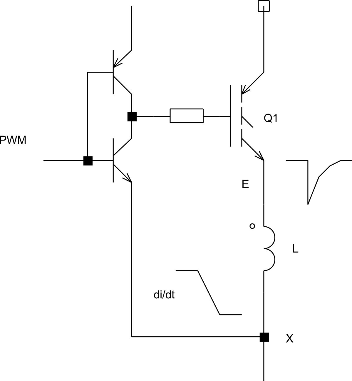
The positive power rail voltage for the gate drive circuit should be high enough to ensure full saturation/enhancement of the power switch without exceeding the absolute maximum voltage for its gate. The MGJ series, for example, has options for +15 or +20V. IGBTs and GaN MOSFETS will be fully ‘on’ with 15V drive but typical SiC MOSFETS may need closer to 20V for full enhancement. In the case of a negative power rail, the off-state, 0V on the gate can be adequate for all devices. However, a negative voltage typically between -5.0 and -10V enables rapid switching controlled by a gate resistor. The on state gate threshold for IGBTs is a few volts, typically 5V but SiC and GaN can be a little over 1V. A consideration also is that any emitter inductance L between a switch and the driver reference, (point ‘x’ in Figure 1), causes an opposing gate-emitter voltage when the switch is turning off. While the inductance may be small, just 5nH would produce 5V at a di/dt of 1,000A/µs which is not unusual - 5nH is just a few mm of wired connection. An appropriate negative drive ensures that the gate-emitter off-voltage is always actually zero or less. The MGJ series offers -5, -8.7, -10 and -15V, depending on variant. A negative gate drive also helps to overcome the effect of collector-gate ‘Miller’ capacitance which works to inject current into the gate drive circuit on device turn-off.

Figure 1: With stray inductance L, on switch-off, negative di/dt produces a negative voltage on the emitter, opposing the turn-off voltage
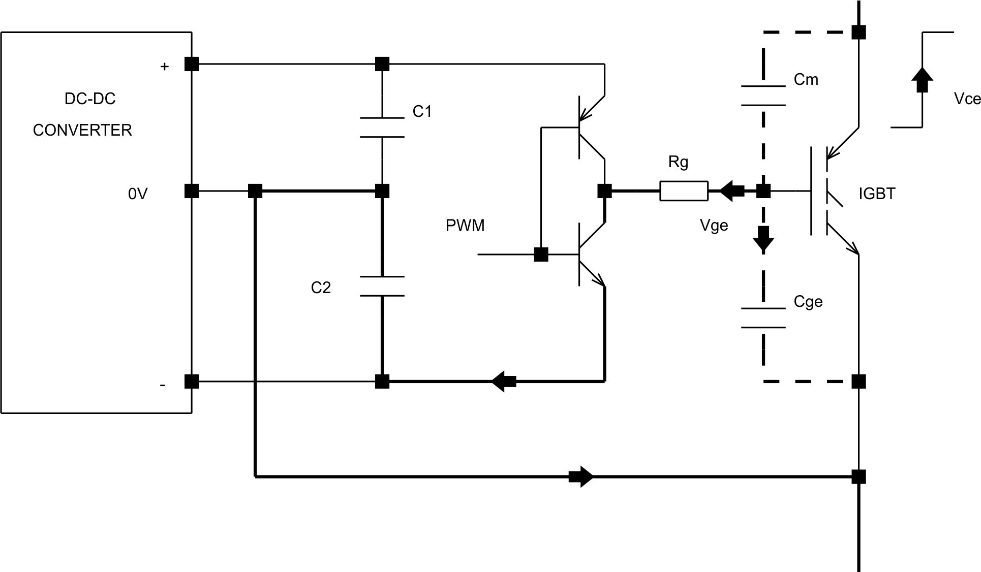
When an IGBT is driven off, the collector-gate voltage rises and dVce/dt flows through the Miller capacitance into the gate emitter capacitance and through the gate resistor to the driver circuit (Figure 2). The resulting voltage Vge on the gate can be sufficient to turn the IGBT on again with possible shoot-through and damage. Driving the gate to a negative voltage mitigates this effect. All types of MOSFETS exhibit the same effect.
Gate power requirements
In each switching cycle, the gate of an IGBT/MOSFET must be charged and discharged through Rg in Figure 2. If the IGBT datasheet provides a gate charge curve then the power dissipated which must be provided by the DC/DC is Qg. F .Vs
Power is dissipated in the internal gate resistance of the device and any external series resistance. If the datasheet does not provide a charge curve but just a Qg value at specific gate voltages, the value at other gate voltage swings can be approximated by multiplying by the ratio of the actual versus datasheet voltage swings. For example, IGBT FZ400R12KE4, from Infineon, has a Qg value of 3.7µC with ±15V gate voltage swing (30V total). For a swing of +15/-10V (25V total) gate charge approximates to: Qg = 3.7e-6 . 25/30 ≈ 3.1 µC
 Figure 2: Current through ‘Miller’ capacitance opposes switch off
At 10 kHz this requires gate drive power of: Pg = 3.1e-6 . 10e3 . 25 ≈ 0.78 W. With derating and allowing for other incidental losses, a 2W DC/DC converter would be suitable. The average current into the gate capacitance must be zero over each switching cycle, therefore the average charge and discharge current in each switching cycle must be the same. The peak current Ipk, required to charge and discharge the gate is a function of Vs, gate resistance of the IGBT/MOSFET Rint and external resistance Rg.
The example IGBT device has Rint of 1.9Ω so with a typical external resistor of 2Ω and a swing of 25V, a peak current of over 6A results. This peak current must be supplied by ‘bulk’ capacitors on the driver supply rails, as the DC/DC converter does not have sufficient value of output capacitors to supply this current without significant ‘droop’. Of course the gate driver itself must be rated for these peak current values, as must the gate resistors. For this example, total gate drive energy E added and removed per cycle is given by:
E = Qg . V s = 75 µJ
The bulk capacitors C1 and C2 (Figure 2) on the +15 and -10V rails supply this energy in proportion to their voltages so the +15 V rail supplies 45µJ. Assume that the bulk capacitor on the +15V rail should not drop more than a small fraction of the rail, say 0.5V each cycle. We can calculate approximate minimum capacitance C by equating the energy supplied with the difference between the capacitor energies at its start and finish voltages, that is: 45 µJ = ½ C (Vinit2 – Vfinal2) C = (45e -6 . 2)/(152 – 14.52) ≈ 6.1 µF
Although the -10V rail supplies about a third of the energy, it requires the same capacitor value for 0.5V drop as this is a larger percentage of the initial value. In practice, the voltage drop may be affected more by the ESR and ESL of the capacitor. For example, an ESR of 0.1Ω would drop more than 0.5V peak at the peak current of 6A. High performance capacitors should be chosen, often necessitating large can sizes to achieve the low ESR, however, maximum capacitances should not be exceeded.
DC/DC regulation
The absolute values of gate drive voltages are not critical as long as they are above the minimum and comfortably below breakdown levels; dissipation is acceptable. The DC/DC converters supplying the drive power therefore may be unregulated types, if the input to the DC/DCs is nominally constant. The load is quite constant when the IGBT/MOSFET is switching at any duty cycle. Alternatively the load is close to zero when the device is not switching. Simple DC/DCs often need a minimum load otherwise the output voltages can dramatically increase, possibly up to the gate breakdown level. This high voltage is stored on the bulk capacitors so that when the device starts to switch, it could see a gate over-voltage until the level drops under normal load. A DC/DC should be chosen that has clamped output voltages or very low minimum load requirements.
IGBTs/MOSFETs should not be actively driven by PWM signals until the drive circuit voltage rails are at correct values. However, as gate drive DC/DCs are powered up or down, a transient condition might exist where devices could be driven on, even with the PWM signal inactive, leading to shoot-through and damage. The DC/DC should therefore be well behaved on power-up and down with monotonic rise and fall times.
Visit Murata Power Solutions: PCIM 2016 - Hall 6-245


