How to specify the optimal heat sink for your design
Excessive temperatures can seriously reduce the lifetime of electronic components. It is well known that for every 10°C rise in operating temperature, the lifetime of an IC is reduced by about 50%.
By: Aaron Yarnell, Senior Product Manager, CUI Devices
As system power densities continue to increase, and sophisticated power-electronics applications continue to proliferate in equipment such as data centers, electric vehicles, lighting systems, industrial robotics and more, thermal management is an increasingly pressing challenge.
While seeking to keep components cool, however, there are many opportunities to 'over engineer', resulting in a solution that is excessively large, or expensive, or both. If the main device for cooling is to be a heat sink, for example, the idea is to choose a part that has optimal thermal impedance (governed by factors such as size, shape, and surface finish) to maintain the device below its rated operating temperature.
Selecting a heat sink: a step-by-step guide
If we consider a simple thermal management challenge, to specify a heat sink for a small device like a power MOSFET in a standard TO-220 package, it is first necessary to quantify the power dissipated by the component. Let’s assume that the total power lost in the transistor due to switching and conduction is 2.7W.
If the sum of thermal impedances between the transistor junction and the ambient air is high enough to prevent this amount of power from being dissipated as heat, continued operation will cause the junction temperature to rise and eventually exceed the maximum permitted device temperature. For silicon transistors, this is typically 125°C.
Is a heat sink needed?
We can first examine whether the MOSFET can operate without a heat sink by referring to the 'junction-to-ambient' thermal impedance (Rθ J-A) quoted in the device datasheet. This is expressed in units of °C/W, and describes how much the junction temperature will rise above the ambient temperature for every Watt dissipated.
A representative value for Rθ J-A of a MOSFET in a TO-220 package is 62°C/W. Hence, in our example, where the device dissipates 2.78W, the junction temperature will increase by 172°C, or 2.78W x 62°C /W. If the ambient temperature is 50°C, this means the junction temperature will rise to 222°C.
Because this exceeds the maximum allowed for the device, we can see that a heat sink is needed. The desired effect is to reduce the thermal impedance between the junction and ambient sufficiently to prevent the junction temperature from exceeding the maximum stated by the manufacturer.
Thermal impedance calculations
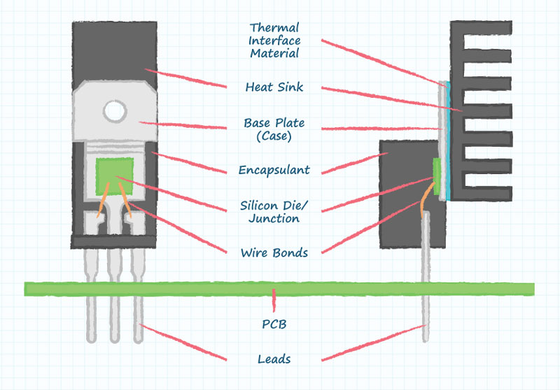
A heat sink is attached to a TO-220 package as shown in figure 1, with the thinnest layer of Thermal Interface Material (TIM) necessary to eliminate air that would otherwise become trapped between case and heat sink due to the imperfect smoothness and coplanarity of the mated surfaces.

Figure 1. Typical TO-220 package with heatsink.
The next step will be to determine the maximum allowable thermal impedance of the entire system, for safe and reliable operation. First, we need to calculate the largest permissible increase in junction temperature. If the maximum allowable temperature is 125°C, and the worst-case ambient temperature is 50°C, the increase can be no more than 75°C.
Next, knowing this figure and the power dissipated by the device, which is 2.78W, we can calculate the maximum thermal impedance of the entire system, comprising the MOSFET package, heat sink, and Thermal Interface Material (TIM) as 75°C ÷ 2.78 W, or 27°C/W.
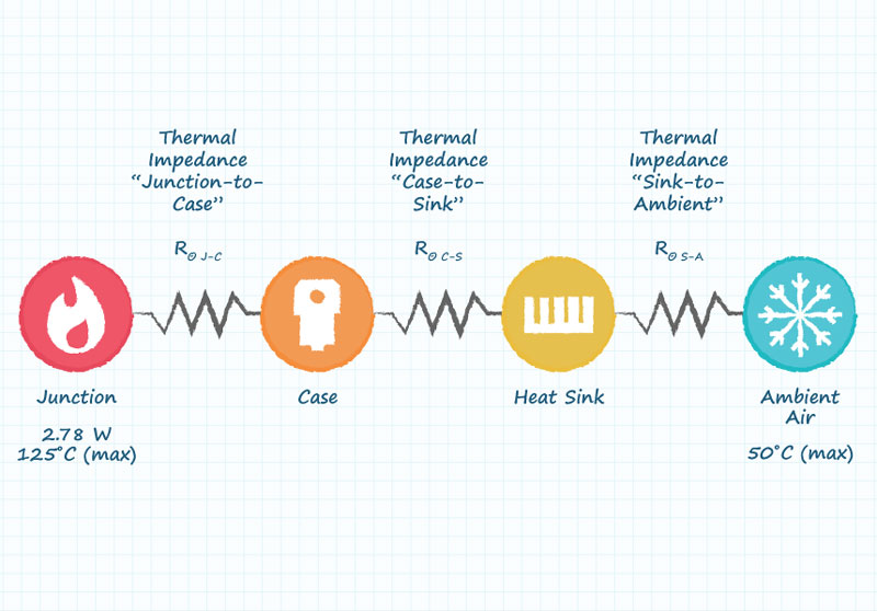
We can model this network of elements as a set of thermal impedances in series (figure 2).

Figure 2. The individual thermal impedances between the junction and the ambient air are added, and compared with the maximum permissible value as calculated.
Factoring in thermal interface materials
The characteristic of the TIM as a material is defined by its thermal conductivity, in units of Watts per Meters-Celsius (W/(m °C)) or Watts per Meters-Kelvin (W/(m K)). The thermal impedance depends on the application, and in particular the layer thickness and surface area. Let’s assume the following for our example:
TIM thermal conductivity ("K"): 0.79 W/(m °C) = 0.79 W/(m K)
TIM surface area: 112 mm2 = 0.000112 m2
TIM thickness: 0.04 mm = 0.00004 m
The thermal impedance can then be calculated:
Rθ C-S = (Thickness / Area) x (1 / Conductivity)
Rθ C-S = (0.00004 / 0.000112) x (1 / 0.79)
Rθ C-S = 0.45 C/W or 0.45 K/W
We previously calculated the maximum allowable thermal impedance between the junction and ambient to be 27°C/W. Now that the impedances from junction-to-case (typically listed on a vendor’s datasheet, 0.5°C/W in this example) and case-to-sink are known, these can be subtracted from this total to show the maximum allowable thermal impedance of a suitable heat sink. Hence, 27°C/W - 0.5°C/W - 0.45°C/W gives a value of 26.05°C/W.
Final calculations to specify the ideal heat sink
The final impedance in the chain, from the heat sink to ambient air, depends on the heat sink’s ability to transfer heat from the surface in contact with the component into the ambient air. Of course, the heat sink is designed to maximise dissipation, with a large, flat surface to be placed against the component.
Dense finning, and often a matte finish, maximise the heat sink’s surface area in contact with the ambient air. Heat sinks for tabbed power packages like the TO-220 are usually either screwed or clipped to the component to ensure reliable and close contact.
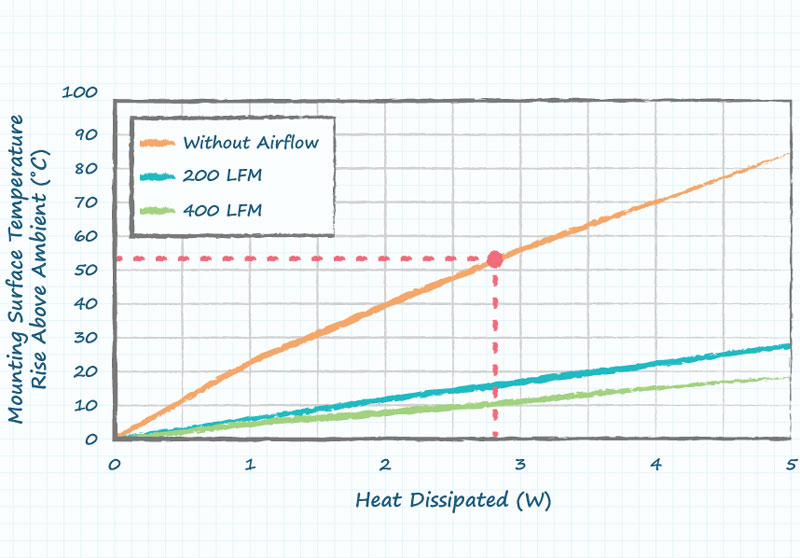
Heat sink vendors like CUI Devices will typically provide graphs (figure 3) or data points to help designers quantify the heat transfer from the heat sink to ambient air under various airflow conditions and loads.

Figure 3. Heat sink datasheet information shows the typical heat sink mounting-surface temperature rise above ambient
Let’s assume the application is operating without airflow, using natural convection only. The graph can be used to find the final thermal impedance (sink-to-ambient) for this particular heat sink. Reading from the graph, when the heat dissipated is 2.78W, the surface temperature rise above ambient is 53°C. The sink-to-ambient thermal impedance can then be calculated as 19.1°C/W by dividing 53°C by 2.78W.
This is comfortably below the 26.05°C/W calculated earlier, showing that the junction temperature will be below the maximum limit by some margin. We can estimate junction operating temperature with this heat sink in place, by adding the thermal impedance of the chosen part to the junction-to-case and case-to-sink values, then multiplying by the power dissipated to find the temperature rise. Adding this figure to the worst-case ambient temperature assumed for the application (50°C), gives the estimated junction temperature:
Estimated Junction Temp. = TAmbient + Watts x (RθJ-C + Rθ C-S + Rθ S-A)
Estimated Junction Temp. = 50 + 2.78 x (0.5 + 0.45 + 19.1)
Estimated Junction Temp. = 105.7°C
This is well below the maximum permissible junction temperature, indicating that the selected heat sink is adequate to prevent the MOSFET from overheating.
View more helpful thermal management resources from CUI Devices and learn more about their line of heat sinks.
Read more helpful How To articles on Thermal Management, Power, Interconnect, Audio, and Motion Control from the CUI Devices' Insights Blog.


