Changing the landscape of computing – 30 years on
A decade before IBM launched the world’s first smartphone, a team of Stanford University researchers and Silicon Valley veterans came together to design a microprocessor architecture that would forever change the landscape of computing. The year was 1986 and the newly formed company was MIPS Computer Systems - a small start-up led by current day Stanford University President John L. Hennessy.
This is the story of MIPS R2000, the first commercially available microprocessor chipset to implement the MIPS instruction set architecture (ISA) and the first RISC processor widely sold through a profitable licensing business model that has become so widespread today.
Risking it all on RISC
Taking advantage of the vast pool of top talent available in Silicon Valley, Hennessy handpicked a team of chip designers, software engineers and computer architecture researchers in the hopes of creating the ultimate RISC processor. Other principal founders included Skip Stritter, formerly a Motorola technologist, and John Moussouris, who came from IBM.
After spending the better part of 1984 putting the final touches on the MIPS architecture, Hennessy and his team officially announced the R2000 in January 1986 - 30 years ago this month.
The MIPS R2000 CPU was a 32-bit design based on the MIPS I architecture that competed with Motorola 68000 and Intel 80386 microprocessors. At the time, MIPS R2000 also faced stiff competition from several other academic projects aiming to create a viable alternative to the more established CISC CPUs of the day.
In order to find a fast way to market and stay ahead of the competition, the MIPS team had to think outside the box - opening a semiconductor fabrication plant (commonly called a fab or foundry) to manufacture MIPS chips was out of the question, given how prohibitively expensive such an undertaking would be.
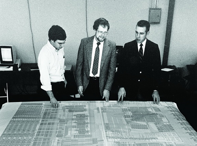
Above: John Hennessy inspecting the layout of MIPS R2000
In order to ensure that its first design made it into production, the management team wisely decided to adopt a fabless manufacturing model. This strategy implied licensing MIPS CPUs to larger semiconductor vendors who had access to a foundry - and would became the norm for other silicon IP designers (including Imagination Technologies) in the decades that followed.
Early licensees for the MIPS R2000 CPU included Integrated Device Technology (IDT), LSI Logic, Performance Semiconductor and DEC. Under the initial agreement, the vendors were free to supply the devices to their direct customers although MIPS itself bought some of the early samples to build reference servers and workstations for development purposes.
Analysing the architecture of the MIPS R2000
MIPS R2000 reached speeds of up to 15MHz and measured 80mm2 in silicon area - the processor contained about 110,000 transistors laid out using a 2.0μm double metal CMOS process node. To put that into perspective, a MIPS-based CPU manufactured in 2015 using a 28nm process can include 24 to 48 high frequency, superscalar cores running at up to 2.5GHz, large and highly associative L1 and L2 caches, and enormous DRAM bandwidth, representing an huge increase in frequency speed and a shrinkage in semiconductor manufacturing processes.
The R2000 microprocessor could be configured to run either in big-endian or little-endian mode. For DECstation workstations, the decision was made to run little-endian to maintain compatibility with both the VAX ISA and the growing population of Intel-based PCs - other companies at the time such as Motorola or IBM were proponents of the big-endian format so having support for both types of endianness was a strategic approach to attract a wide customer base.
One of the major new features of the R2000 chip was the fast execution time in the absence of cache misses - it delivered an instruction completion rate of one instruction per ALU cycle in an era where non-RISC microprocessors needed several cycles per instruction.
Since the MIPS architecture quickly became popular with workstation and server manufacturers, having good floating point performance was an absolute requirement. To address the need for increased math performance, the engineering team designed an external floating point unit called the R2010 in mid-1987 - in addition, a four stage R2020 write buffer improved performance by permitting the R2000 CPU to write to its write through data cache without stalling.
See MIPS run
One of the factors that significantly contributed to the rapid adoption of the MIPS architecture was the work done by the compiler team on software optimisation. Since the engineers didn’t have access to a real MIPS-based device until late 1986, they built a fast simulator that translated MIPS instructions into native VAX code - this simulator was also used to run UNIX software binaries on the MIPS architecture.
There are currently many MIPS simulators available to software developers, including QuantumLeap from Imperas or the open source QEMU simulator - to name a few.
Where is MIPS now?
In 1988, MIPS Computer Systems released the R3000 processor which used a similar overall system design but provided faster speeds by adding memory management and cache facilities. MIPS R3000 was a popular CPU, finding its way into many workstations and servers from SGI, DEC, Evans & Sutherland as well as the original Sony PlayStation game console.
Right now, a MIPS R3000 CPU is also guiding the NASA New Horizons probe to the Kuiper belt after having completed a flyby of Pluto earlier in September.
Over the years, the MIPS architecture continued to develop with the MIPS II, MIPS III, MIPS IV and MIPS V ISAs. There are presently two main ISAs in use (MIPS32 and MIPS64) scaling from the smallest microcontrollers used in embedded applications to many core, high performance CPUs used in high end networking devices or semi-autonomous cars.


