How memory improvements will expand embedded storage
With mobile product shipments, dominated by smartphones, continuing to account for a significant amount of the non-volatile memory (NVM) market, suppliers and standardisation organisations are working hard to ensure that next-generation NVMs keep up with the demands placed upon them.
Author: Axel Stoermann, Toshiba Memory Europe
Analysts predict compound annual growth rates (CAGR) of up to 10% in the year to 2022, with the NVM market forecast to reach $82 billion in size, and smartphones contributing to a quarter or more of this growth.
With smartphones such an integral part of our lives, handling activities from messaging and email, to gaming and video, existing memory architectures and interfaces are proving to be a bottle neck, negatively impacting the user experience.
As one example, activities that should be independent of one another, such as installing an update and playing a video, can impact each other due to limitations in the speed and scheduling of data transfers between processor and NVM. This results in undesired side-effects, such as juddering video and skipped audio.
In this white paper we examine what improvements memory technology will provide, and how next generation embedded flash-memory interfaces will complement these technological advances.
NVM is growing up
Whilst other semiconductor applications can look to ever smaller process nodes to achieve smaller, faster, better, simply compressing more components onto each square millimetre of die space is a mixed blessing for flash memory. In the 30 years since Toshiba invented flash memory, bit densities have increased 2000-fold through progressive innovation and implementation of new technology nodes. Lithographic scaling has dropped process nodes sizes from 350 nm down to 15 nm, while moving to larger wafers, packaging innovation and increased automation has driven down prices, increased capacity per chip and delivered optimisations in package volume. It is safe to say that NVM innovation has significantly contributed to the success of the slim line, power efficient smartphones we all carry today.
In first generation flash memory, each memory cell was used to store a single bit of information. These were termed Single Level Cell (SLC) architectures. In order to achieve higher memory densities for the same die area, bit densities were doubled to two bits per cell, known as Multiple Level Cell (MLC) devices. This was achieved by storing the data as one of four different voltage levels, with each level coded and being assigned the value ‘00’, ‘01’, ‘10’ and ‘11’. With pressure to achieve even higher densities, technology progressed to support Triple Level Cells (TLC), storing three bits of data per cell.
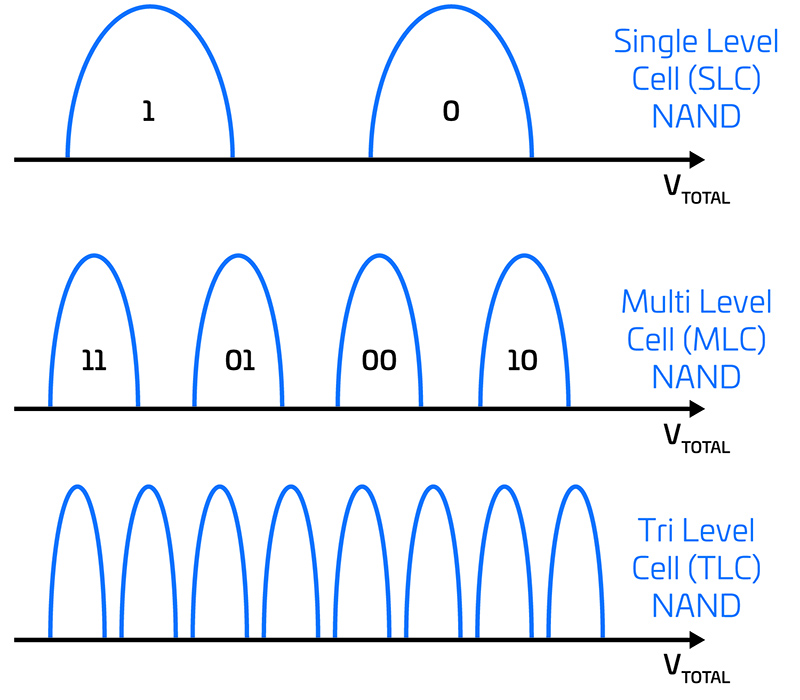 Figure 1: SLC NAND stores a single bit per cell; by increasing the number of different coding voltages stored per cell, more bits per cell can be achieved
As it is always the case, such leaps in performance cannot be achieved without compromise. The technology required to write different voltage levels, and determine the correct level when reading, result in more wear on the individual cells and additional circuitry to handle bit errors. In turn, the lifetime, or read / write cycles per cell, drop significantly with the move from SLC through MLC to TLC technologies. In some applications, this is not such an issue, since the number of read / write cycles offered by SLC were not being reached. In many applications, high reliability is only required for a specific section of the application code, such as the bootloader. MLC and TLC NAND memories frequently offer a partitioning option, allowing a high-reliability section of memory to function in SLC mode (named pseudo SLC or pSLC), at the expense of reduced memory capacity, since only one bit of data per cell is stored.
The move to add more memory capacity in volume, rather than purely across the area of the die, has led to the development of 3D structures. With room to grow vertically, there is less need to work at the tiniest of process nodes. Thus, Toshiba’s 3D NAND flash memory technology, BiCS (bit column stacked), returns to larger lithographic processes, reversing the trend for die shrinking, in favour of an increased cell spacing that reduces cell-to-cell noise and interference. The technology also moves away from the traditional doped polycrystalline silicon of planar NAND flash technologies, instead favouring a silicon nitride layer of charge trap cells.
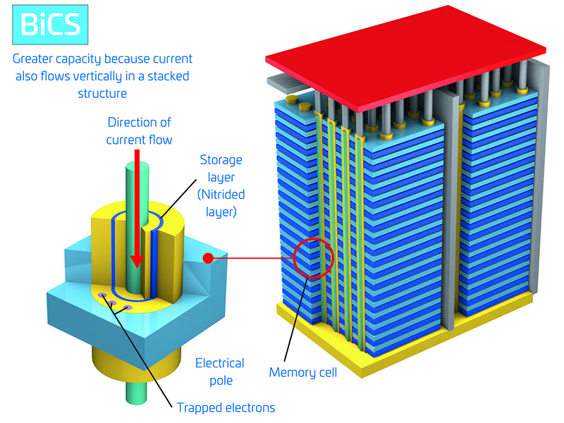 Figure 2: BiCS NAND structure uses a silicon nitride layer of charge trap cells
With a 96-layer structure, memory density is delivered a quantum leap in growth. With more inter-cell spacing, read / write endurance is significantly improved, lower voltages deliver enhanced power efficiency, and write speeds increase. As a reference point, a typical 2D NAND can currently support sequential write speeds of 20-30 MB/sec. By comparison, the latest generation of 3D BiCS memories now achieve 30-40 MB/sec. This equates to a data transfer speed of over 500Mbps.
These improvements are made possible because of the significantly higher number of electrons that can be stored in a 3D BiCS cell in comparison to a 2D, 15nm floating gate cell (Figure 3). As a consequence, the endurance of a BiCS cell is generally higher than for a floating cell. A typical BiCS/TLC cell has the same as the endurance as a 2D/MLC cell. This opens up the possibility for a BiCS/QLC (storing four bits in one cell), which will have comparable endurance to 2D/TLC.
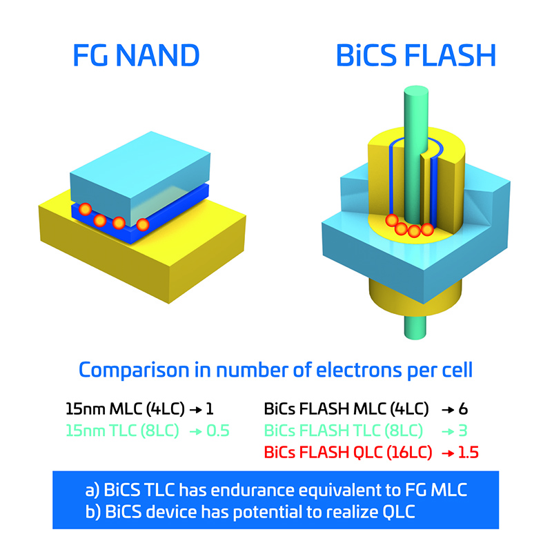 Figure 3: Comparison of the relative number of electrons stored in a floating gate compared with a BiCS cell
Along with 3D structures being used for the silicon itself, stacked die technology was also being employed to increase the amount of storage in the device package. Using Die Attached Film (DAF), die of increasingly smaller area are stacked on top of one another, with pads being wire bonded to the lead frame of the package. Such long leads are challenging to bond and were proving to be a bottle neck in data transfer speeds.
By collaborating with the New Energy and Industrial Technology Development Organisation, innovative new ways of inter-die bonding were developed. This collaboration resulted in Through Silicon Via (TSV) technology, allowing die of equal size to be stacked upon one another, and the individual 3D BiCS flash memory die to be bonded to one another and the packaging without traditional bonding wires. These shortened electrical pathways, and the resulting reduction in parasitic components, has resulted in further reductions in power consumption coupled with further increases in data transfer. TSV bonded 3D BiCS is capable of achieving speeds of over 1 Gbps, around double that of the wire-bonded versions of original BiCS memory devices.
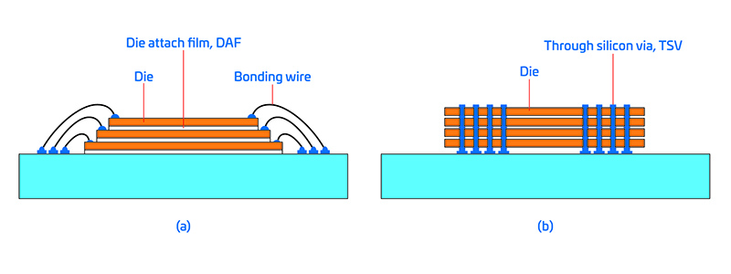 Figure 4: TSV significantly reduces parasitics compared to wire bonding, delivering further data transfer speed improvements
Acquiring the data transfer speed gains
With NAND flash technology having overcome the significant hurdles that were limiting capacity growth and transfer speed, the interface to the memory has become the bottle-neck once more. Historically evolved from the Multimedia Card (MMC), the embedded Multimedia Card (eMMC) standard has focused upon ensuring that there is a memory format suitable for the wide range of portable electronic consumer products we have today.
The standard defines the interface, the protocol and even the packaging of flash memory, allowing OEMs to select and switch between suppliers as market needs impact supply and demand. The interface is parallel, consisting of 1, 4 or 8 bits along with a clock pin and a bi-directional command interface. In order to simplify the software and hardware of the host processor, the specification also defines functionality to ensure the reliable device operation of the memory in the application over time. This housekeeping includes error-correction (ECC), garbage collection, wear levelling and bad block management. This ensures data integrity for the user, while allowing embedded software developers to focus on using the medium for storage rather than having to tend it as well.
The eMMC JEDEC standard has continuously developed to meet industry, and indirectly consumer demands with the introduction of features to determine the health of the storage medium, provide support for queueing and reordering of commands, and offer more control over background operations that would otherwise impact time critical read / write activities. A dual data rate operating mode has also increased transfer speeds. However, the parallel interface, at 400 MB/s transfer speeds, is now outperformed by the read speed modern NAND flash memories can offer.
Further limitations with eMMC concern its half-duplex topology, limiting it to either reading or writing, but not both simultaneously. In today’s world of multicore, multithreaded applications, this can cause significant issues. A typical smartphone is continuously accessing NVM to retrieve data for apps or to play videos, whilst attempting to write updates to databases or store photos. Power consumption is also a challenge, something that is difficult to keep under control as parallel digital interfaces increase in speed.
Partitioning of memory is another area for improvement. Typically, a boot partition is required to prepare the SoC to execute a high-level operating system. These can be implemented as virtual partitions, with the boundaries notionally defined by the file system. However, at hardware level, to ensure reliability, it may be considered prudent to switch from MLC or TLC operation to pSLC for this partition. As time passes, it could occur that, as a result of bad blocks or wear levelling, blocks belonging to this partition are moved from higher-endurance pSLC areas to lower-endurance MLC or TLC areas, thus negating the advantages of the chosen improved endurance location.
With the eMMC standard coming toward the end of its useful life, the same working group developed a new standard that would provide room to overcome the limitations of eMMC, both now and in the future. That standard is Universal Flash Storage (UFS). UFS is tailored to the needs of flash as a storage medium, while leveraging the advantages of other popular storage interfaces and protocols, such as the former MIPI (eMMC) and SCSI standards.
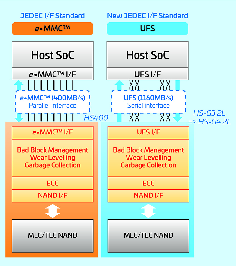 Figure 5: The eMMC interface is limited to 400 MB/s; this is compared to the gigabit performance of the UFS standard
The first obvious difference is the choice of physical interface resulting in a lower pin count as well. UFS makes use of the MIPI and UniPro standards for the physical and link layers. This provides multiple lanes of high-speed serial interfaces that are also energy efficient. The MIPI M-PHY standard defines different ‘gear’ speeds, with gear 1 supporting 1.46 Gbps and gear 4 supporting 11.6 Gbps. The interface also supports asynchronous data transfers and low power sleep modes.
Partitioning is another area of improvement, with UFS allowing the storage medium to be split into multiple device-level partitions. The partitions can also be configured to leverage the maximum storage capacity of the flash (TLC mode) or maximum endurance (pSLC mode). System data, such as boot code and the operating system, is then guaranteed to always have access to high-endurance memory when demanded by the application.
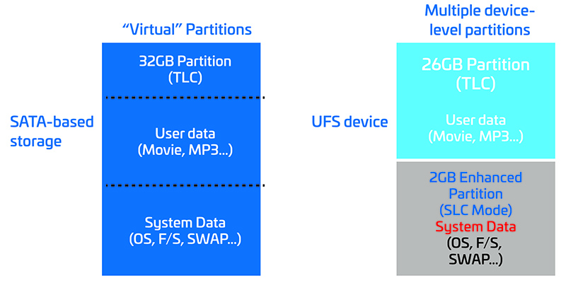 Figure 6: The UFS standard allows physical partition on the storage medium, guaranteeing endurance where the application demands it
Partitions can also be assigned different level of performance. As an example, features surrounding photos and video frequently differentiate smartphone offerings, so it is imperative that images and video can be stored to NVM as quickly as possible. Any updates to the operating systems, databases or apps can be considered to be of a lower priority. With prioritised partitions, UFS’ intelligent command queueing capability ensures that urgent memory accesses, such as saving an image, are given priority over less time-critical accesses, such as app updates.
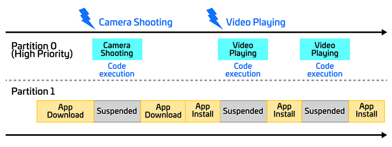 Figure 7: Assigning a priority to a partition ensures that storage of user data can interrupt system-level memory updates
Storage accesses in many applications can be broadly split into those that are sequential, such as playing videos or music, and those that are random, such as web browsing, switching between apps, booting and reading email. Multitasking operating systems can therefore be expected to need to require simultaneous read and write accesses that are efficient both for sequential as well as random data accesses. UFS also supports this, by offering full duplex and dual multi-page programming across multiple lanes.
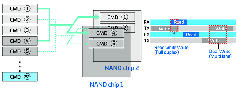 Figure 8: The biggest improvement UFS delivers is full-duplex memory access
How vertical markets will adopt the changes
Any change in technology takes time to work its way through to the end consumer. As a result, eMMC will continue to be the memory of choice for a wide range of applications. This is due to the performance being adequate for low to medium end applications, and the interface being supported by current and older generations of SoCs. Until now traditional markets, such as automotive, have relied upon eMMC due to it being a known quantity, adequately fulfilling the needs of their applications and being automotive qualified.

Figure 9: Each market will move to UFS at the moment when the gains add significant value-add over eMMC memories
However, it will not be long before the SoCs used in automotive favour UFS over eMMC. Increasingly demanding applications in the automotive segment will also drive the need to leverage the data-throughput performance and improved feature set that UFS offers (e.g. support of multithreaded applications). Transitioning to 3D BiCS memory at the same time will deliver high capacity, power savings and an increase in robustness and endurance compared to current memory offerings.
Conclusion
One thing is certain – eMMC is not about to fade away immediately. Too many markets with slow replacement cycles, and reliability and functional safety concerns, depend on this robust and well-understood technology to change any time soon. For some applications, it quite simply still does the job it was intended to do. However, as SoCs replace eMMC support with UFS, the moment will arrive to consider changing both the memory interface and memory technology in one go.
3D BiCS technology, with its stacked topology, and larger lithographic processes compared to planar type flash technologies, enable significant increases in memory density coupled with higher endurance, and improvements in reliability, performance and power efficiency. When coupled with the capabilities of the latest UFS standard, developers have access to a high-speed memory platform that meets the needs of embedded designers both now and for the foreseeable future.


