ESD protection for automotive high-speed video links
Autonomous driving is one of the big trends predicted to change the future of the automotive industry. Its successful adoption is dependent on overcoming barriers such as the need for more safety and information for the driver and the passengers. This in turn is driving the development of Advanced Driver Assist Systems (ADAS) and safety infotainment applications for use in future autonomous vehicles.
Due to this trend, the number of cameras and displays in a car’s interior is multiplying rapidly. While Video Links provide adequate data rates (up to 16Gbits) to satisfy the need for quality content, vehicles still a rough environment for those sensitive interfaces. The physical layer (PHY) technology for such highly sophisticated links requires external electrostatic discharge (ESD) protection that is compliant with the automotive electromagnetic compatibility (EMC) requirements. For the ESD protection itself, this introduces some new challenges. On the one handthe ESD device should protectthe circuit against high voltage ESD events. On the other hand ESD device should be mostly invisible during normal operation, havindg no significant impact on the signal integrity (SI). Besides package and routing, the main intrinsic parameter for SI compliance is the capacitance of the ESD device. As data rates rise, the demand for lower capacitance grows.
This paper discusses the impact of the ESD protection device on SI in comparison to other link components such as cable, connector and the PCB in a differential video link. Therefore the entire link from Rx to Tx is built up in ADSand scattering parameters simulation is performed.
Video links
Video Links, or serialiser/deserialiser (SerDes), are umbrella terms for devices using serial interfaces to transmit data that is available from a parallel data stream. These interfaces are high bandwidth, point-to-point by design, and latency is usually not critical. The interfaces mainly operate unidirectionally or bidirectionally where the bandwidth in one direction is significantly higher than in the other. The physical implementation of the serial data stream can be differential, using low voltage differential signaling (LVDS), or single-ended, using a coaxial cable. (Optical links are also possible, but they are not standard and therefore will not be discussed here.) Furthermore, Video Link interfaces with a single-ended physical layer are sometimes used to transmit power to the ECU in addition to the data stream. For coaxial single-ended links, this technique is called Power-over-Coax (PoC) in the same vein as Power-over-Data-line (PoDl) or Power-over-Ethernet (PoE).
Video Link interfaces are mainly used to transmit video data. The most common applications are in infotainment to connect displays, body and convenience applications like parking cameras, and cameras used for ADAS applications. Especially for cameras, the PoC functionality is very attractive. In the modern zonal architecture, Video Link interfaces are the exceptional point-to-point connections that are required to make high-resolution sensor data available. There is an initiative ongoing to standardize Video Link interfaces for automotive applications, but currently no common standard is available. Proprietary solutions are therefore common in the automotive domain, such as the following examples.
APIX – Automotive Pixel Link
Automotive Pixel Link (APIX) was designed by Inova Semiconductors and licensed in 2008 by Fujitsu. It can be used to transmit digital video signals over a distance of up to 15m. Third generation APIX3 has been available since 2016, suppling data rates up to 6Gbit/s.
GMSL – Gigabit Multimedia Serial Link
GMSL is a proprietary SerDes interface by Maxim Integrated mainly used for camera applications. The third generation of increases the data rate beyond 10Gbit/s range supporting also PoC as an option.
FPD-Link – Flat Panel Display Link
FPD-Link was originally designed for displays but is also commonly used to connect cameras to ADAS computing units. Today, FPD-Link is owned by TI and very popular for automotive ADAS applications. FPD-Link III allows for data rates of up to 13.3 Gbit/s and bi-directional communication on a single link. Additionally, FPD-Link III allows the usage of coaxial cables and PoC in a single-ended variant.

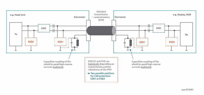
Figure 1: Schematic of a differential video link including the transceiver and receiver
ESD requirements for video links
The requirements for external protection are similar for all three video link interfaces introduced in the previous section. As mentioned previously, there are two main parameters topics to be focused on when choosing the right ESD protection device, ESD and SI. Both will be addressed in the following.
To achieve ESD protection up to 10kV or more and to have a very robust system in the field, state-of-the-art protection technology is required – such as a silicon-controlled rectifier (SCR) or open base transistor. As illustrated in Figure 1, there are two possible positions for an ESD protection device: ESD1 and ESD2. For optimal ESD protection performance, the position to choose is the ESD1, which allows the ESD pulse to be clamped down directly at the connector, far away from the sensitive PHY and the circuitry. Typically, in automotive testing a ‘short to battery’ is also performed for video links. In this case the ESD1 position can be populated, which requires the reverse standoff voltage (VRWM) of the ESD protection device to be above 13.5V. If short to battery is not tested, then a VRWM of 5V or lower can be chosen. Position ESD2 is not impacted by the short to battery test since the DC capacitors are blocking the DC current. Here, lower standoff voltages of of 5V or below can be used. In some cases, capacitive coupling of the shield of the cable is required and can be considered as a possible ground reference for the ESD protection device.
Today’s infotainment in automotive requires a high resolution and high-quality video stream. Hence, the data rate of video links is increasing rapidly. With the new generations of video links, a data rate of up to 13Gbps is state-of-the-art and will increase to 16Gbps in future. In such scenarios, signal integrity plays a key role for design engineers.
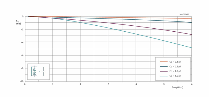
When choosing an ESD protection device with SI focus there are several parameters to consider. During normal operation the voltage across the ESD protection device is very small usually below 1V. In this case, the ESD protection device behaves as a capacitance parallel in the signal transmission path. This device capacitance Cd is one of the most important parameters for the SI. Due to the high data rates upt to 16Gbit/s, very low values Cd <1pF are key here. The general effect of such a capacitance on S-parameter is shown in Figure 2 up to 6GHz.

Figure 2 Insertion loss versus frequency for typical device capacitance values. Values below 1.1pF have nearly no impact on the signal transmission
Capacitance values below 1pF clearly stay above the 3dB limit, even above 1dB for 0.5pF. So, in general, values below 1pF or even below 0.5pF allow very good signal transmission up to 6GHz.
In addition, the package and its impact on routing of signal lines may have a significant impact on the signal integrity. As a general rule, the best choices are compact and leadless packages such as DFN (dual-flat no leads), which are generally less parasitic compared to leaded ones. In addition, they usually have a very compact footprint with only a minor impact on the routing of the signal lines, hence, on their the impedance. So, the capacitance of the ESD protection can be seen as a dominant value.
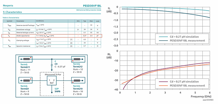
Figure 3 shows the comparison of capacitance in a simulated device with a measurement of a real ESD protection device PESD30VF1BL. Here, the typical value of Cd = 0.27pF from the datasheet was used for the simulation. This product is a tiny leadless Surface-Mounted Device (SMD) plastic package designed to protect one signal line from the damage caused by ESD and other transients. Both, insertion loss (IL) and return loss (RL) show a good comparison up to 6GHz, demonstrating that device capacitance gives a very good indication for signal integrity purposes.

Figure 3 S-Parameter simulation of a device capacitance of Cd = 0.27pF and a comparison with measured S-Parameter from a real device. Good agreement can be obtained up to 6GHz
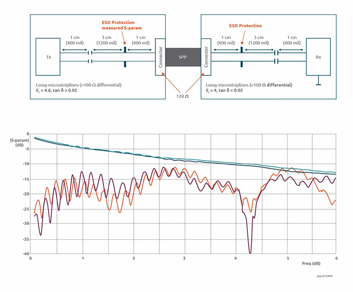
To investigate the impact on the signal integrity of the entire link, including serializer (Tx) and deserializer (Rx), the entire PCB board and cable transmission was simulated in ADS, see Figure 4. The PCB was simulated using lossy microstrip lines of 100Ω. As a substrate a typical FR4 with εr=4.6, tanδ = 0.02 was used. Ideal 100nF capacitors were chosen as DC block. The cable is represented by the measured S-parameter of a typical shielded parallel pair cable (SPP) with a length of 10m. The connector was simulated by a mismatched microstrip line of 120Ω. In reality, the impedance of the connector is very strong dependent on the PCB stack-up and the layout, and it can range from 60 to 150Ωor more which can be very critical for the entire signal transmission.
In order to investigate the impact of the ESD protection device, the measured S-parameter of the Nexperia PESD30VF1BL was used. This device comes with a typical capacitance of 0.27pF and a very compact and leadless package (SOD882BD). It should be mentioned that in this set-up the PCB routing aspects are not considered here, due a very compact package and its minor impact on the SI. Figure 4 shows the comparison of S-parameters (IL and RL) of the entire link from Tx to Rx with and without the ESD protection device. It can be observed that the cable, the connector and the PCB are the most dominant here. The contribution of the ESD protection device is of less importance.

Figure 4: a) Set-up for the link simulation in ADS to investigate the impact of an ESD protection device on the differential S-parameter. b) The impact of the ESD device is minor compared to other components in the link, e.g. cable or connector
Conclusions
The exploding demand of infotainment and safety in modern car systems requires very sophisticated high-speed solutions which pass the EMC compliant test and are robust in the field. ESD can cause a malfunction or even irreversible destruction of the system which is a reason for costly recall campaigns. ESD protection devices are necessary to avoid those failures and leverage the system to a highly reliable and very robust level.
Besides the existing video link protocols, the are some alternatives under discussion within the automotive industry. An open committee, Automotive Serdes Alliance, has been formed to create a common standard for high-speed video links, which will give further assurance of their reliability and performance.
In the meantime, tests demonstrate that Nexperia’s automotive qualified devices for infotainment designs offer the ideal combination of low capacitance, low clamping voltage and high ESD robustness. They use the same active silicon-controlled rectification technology to overcome the traditional protection trade-off challenge. As a result, capacitance is kept down to 0.5pF, clamping voltage is just 3V and devices can withstand surge and ESD pulses up to 10A 8/20µs. In addition, these ESD protection devices comply with all automotive qualifications in a very compact and suitable high-speed package.


