High power density systems demand high current converters
Steve Knoth, Senior Product Marketing Engineer, Power Products at Linear Technology now part of Analog Devices discusses here how high power density systems demand high current converters. The expanding market for high current, low voltage digital ICs reached $9.2bn in 2016. This group of digital ICs includes microcontrollers and microprocessors (µC & µP), programmable logic devices (PLDs), digital signal processors (DSPs), application specific integrated circuit (ASICs), programmable logic devices (PLDs) and graphics processor units (GPUs).
Furthermore, looking at the projections for a big subset of this market – Field Programmable Gate Array ICs (FPGAs) – this segment was valued at $3.92bn in 2014 and is expected to reach $7.23bn by 2022, with a CAGR of 7.41% between 2016 and 2022. High power density digital ICs have penetrated into virtually every embedded system. These systems include, but are not limited to, industrial, communications, telecom, servers, medical, gaming, consumer audio/video and automotive.
FPGAs are enabling cutting-edge applications to come to fruition within these market segments, for example in automotive applications to remove human errors, such as advanced driver assistance systems (ADAS) and collision avoidance systems. Moreover, government–mandated safety features such as anti-lock brake systems, stability control and electronically controlled independent suspension systems have necessitated the use of FPGAs. In the consumer electronics sector, the demand for Internet of things (IoT), machine to machine (M2M) and the growth of data and server centers driven by the demands of large data storage and cloud computing are some of the factors also driving the FPGA market.
These high power density digital IC-based systems have a unique set of power requirements. The combination of high current, low voltage and fast transient response for this current generation of FPGA and ASIC processors place ever more stringent demands on the power supplies that power the device. These digital ICs are powerful, yet temperamental from a power standpoint. Traditionally, efficient switching regulator controllers with separate high power MOSFETs have been used to power these devices but they have exhibited potential noise interference issues, slower transient response and layout limitations. As a result, in recent years low dropout regulators (LDOs) that minimise heat have been used as an alternative, but not without their own set of limitations. However, thanks to recent product innovations in this area, the trend is changing. Newer high power monolithic switching regulators no longer come with performance tradeoffs and are rapidly finding their way into these applications.
Switching regulators vs charge pumps & LDOs
Low voltage high current step-down conversion and regulation can be achieved via a variety of methods with a variety of design tradeoffs. For starters, switching regulator controllers operate with high efficiency for high currents over a wide range of voltages but require external components such as inductors and capacitors (and FETs in the controller case) for operation. Inductorless charge pumps (or switched capacitor voltage converters) can also be used to achieve lower voltage conversion but are limited in output current capability, suffer from poor transient performance and require more external components versus a linear regulator. As a result, charge pumps are not commonly found in digital IC power applications. Conversely, linear regulators and especially LDOs are simple in that they only require 2 external capacitors to operate. However, they may be power limited depending on the size of the input to output voltage differential across the IC and how much current is demanded by the load, plus the thermal resistance characteristics of the package. This limits their penetration into powering digital ICs.
High current monolithic buck converter design challenges
Closely following Moore’s Law (originally conceived in 1965), wafer fabrication technology line widths are ever decreasing, therefore requiring lower voltage operation of digital ICs. Smaller geometry processes allow higher integration of more power-hungry features in the end product. For example, modern computer servers and communication routing systems demand higher bandwidth to process more computing data and internet traffic. Cars have more on-board electronics for entertainment, navigation, self-driving features, and even engine control. As a result, system current consumption and associated total power required increases. Therefore state of the art packaging and innovative internal power stage design are required to drive the heat out of the power IC while delivering unprecedented power.
The requirements for high power supply rejection (PSRR) and low output voltage noise or ripple are two additional challenges which also need consideration. A device with high supply rejection can more easily filter and reject noise at the input, resulting in a clean and stable output. Further, a device with low output voltage noise across a wide bandwidth or low output ripple is beneficial to power today’s modern low-noise rails where noise sensitivity is a major design consideration. As the speed requirements for high end FPGAs increase, the supply noise tolerance continues to decrease in order to minimise bit errors. These noise-induced digital faults drastically reduce the effective data throughput speeds for these high speed PLDs. Input supply noise at high currents is clearly an important but demanding specification.
Higher transceiver speeds – in FPGAs for example - dictate higher current levels due to higher power consumption from fine geometry circuit switching. These ICs are fast – they may cycle load current from near zero to several amps in tens to hundreds of nanoseconds, requiring a regulator with ultrafast transient response.
With board area reserved for the power regulators ever decreasing, it is well known that a monolithic switching regulator with fast switching frequency reduces the size of external components and therefore total solution size, with a tradeoff of some minor loss in efficiency due to switching losses at higher frequencies. However, a new generation of monolithic switching regulators provides features that significantly reduce the amount of switching losses even at higher frequencies. Namely, synchronous operation with integrated high and low side switches allows for better control of their gate voltages which greatly reduces dead-time thereby resulting in higher efficiency operation.
One of the biggest challenges with high current monolithic switchers is their ability to dissipate heat resulting from significant power loss in the IC. This challenge is met by using thermally enhanced ball-grid array (BGA) packages where the majority of the solder balls are dedicated for power pins (VIN, SW, GND), such that the heat can be easily transferred from the IC into the board. The large copper planes on the board connecting to these power pins allows for the heat to spread more evenly.
New high current buck converters
It is clear that a buck converter solution which solves the issues outlined herein needs to have the following attributes:
- Fast switching frequency – reduces size of external components
- Zero dead-time design - for increased efficiency
- Monolithic – onboard power devices for smaller solution size
- Synchronous operation – higher efficiency and reduced power loss
- Simple design - minimal external components required
- Very low output ripple
- Fast transient response time
- Operation over a wide input/output voltage range
- High output current capability
- Excellent thermal performance
- Compact footprint
To address these specific needs, Linear Technology introduced the LTC71xx family of monolithic high current buck regulators. The newest member is the LTC7150S, a 20V / 20A monolithic synchronous buck converter with differential VOUT remote sensing. The device’s phase lockable controlled on-time constant frequency current mode architecture eases compensation and is ideal for high step-down ratio applications that operate at high frequencies while demanding fast transient response. The LTC7150S uses Silent Switcher 2 technology, including integrated bypass capacitors to deliver a highly efficient solution at high frequencies with excellent EMI performance.
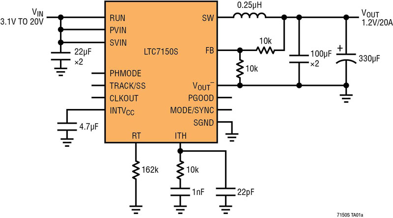
Multiphase operation - up to 12 phases - provides the capability to directly parallel multiple devices for higher current with minimal input and output capacitance. VOUT remote sense ensures that voltage regulation at the load is accurate regardless of load current or board layout. Its wide 3.1-20V input range supports a wide variety of applications, including most intermediate bus voltages and is compatible with many battery types. Integrated N-channel MOSFETs deliver continuous load currents as high as 20A with minimal thermal derating at output voltages spanning from 0.6V to VIN, ideal for point-of-load applications such as high current/low-voltage DSP/FPGA/ASIC reference designs. Other applications include telecom/datacom systems, distributed power architectures and general high power density systems. Figure 1 shows a typical application schematic exhibiting the simplicity of the design.

Figure 1. LTC7150S Typical Application Schematic (7150 TA01a)
The LTC7150S’s very low 25ns minimum on time allows for a high step-down ratio power supply at high frequency operation. The operating frequency is user-selectable from 400kHz to 3MHz and can be synchronised to an external clock. The LTC7150S’s total differential output voltage accuracy is ±1% over the –40 to 125°C operating junction temperature range. Additional features include a high speed differential remote sense amplifier, PHMODE phase selector pin, accurate 1.2V RUN pin threshold, VIN overvoltage protection, Power Good and programmable soft-start/tracking.
Lastly, the LTC7150S is available in a thermally enhanced 42-lead 6×5×1.3mm BGA package, both RoHS lead-free and leaded SnPb (63/37) finishes. The E and I grades are specified from –40°C to 125°C junction operating.
High efficiency, reduced EMI & fast transient response
The “S” in the LTC7150S part number refers to the second generation Silent Switcher technology. The IC has integrated ceramic capacitors for VIN and BOOST to keep all the fast AC current loops small, thus improving the EMI performance. Furthermore, it allows for faster switching edges, which greatly improves efficiency at high switching frequencies.
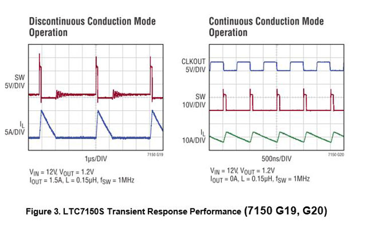
The LTC7150S’s controlled on-time architecture allows the IC to respond to transient steps rapidly. This is accomplished during the transient step - the switching frequency inherently speeds up which allows the inductor current to better shadow what the output of the Error Amplifier (ITH) wants it to be. This allows the ITH compensation to be set more aggressively, increasing overall loop bandwidth.
One key feature of the LTC7150S that allows for high efficiency at high frequencies is the significant reduction of dead time. A servo loop inside the IC locks the dead-time before the SW rising edge to <1ns. The reduced dead time minimises/eliminates the need for body diode conduction of the bottom switch. This essentially eliminates the effect of the reverse recovery of the bottom switch body diode as top switch turns on. The reduction in power loss with this feature is quite significant.
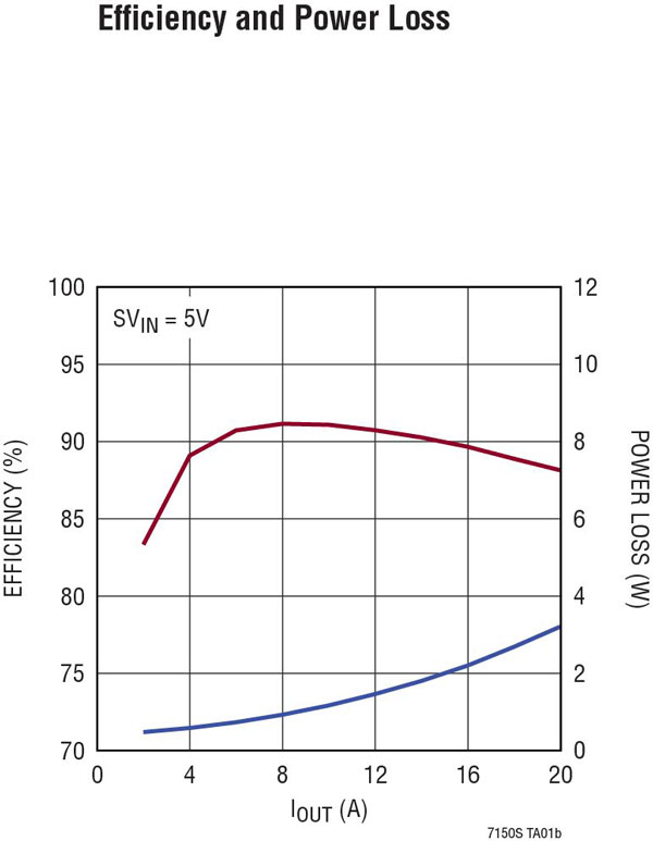
Lower ripple current reduces core losses in the inductor, ESR losses in the output capacitors and output voltage ripple. High efficiency operation is obtained at low frequency with small ripple current. However, achieving this requires a large inductor. There is a trade-off between component size, efficiency and operating frequency. The graph in Figure 2 shows the LTC7150S’s high efficiency performance.
The constant frequency/controlled on-time architecture is ideal for high step down ratio applications that operate at high frequencies while demanding fast transient response. Figure 3 shows the LTC7150S’s transient response performance.

Figure 2. LTC7150S Efficiency Performance (7150 TA01b)

Figure 3. LTC7150S Transient Response Performance (7150 G19, G20)
Ultralow DCR current sensing applications
The LTC7130 is a constant frequency peak current mode control synchronous step-down DC/DC converter with temperature-compensated ultralow DCR current sensing and clock synchronisation. The device’s architecture eases compensation and offers the ability to directly parallel it for higher output current capability. It also enhances the signal-to-noise ratio of the current sense signal, enabling the use of a very low DC resistance power inductor to maximise efficiency in high current applications.
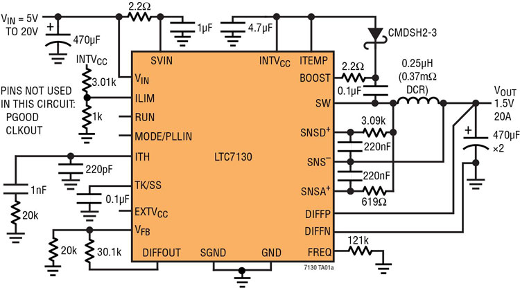
This feature also reduces the switching jitter commonly found in low DCR applications and improves current limit accuracy. The LTC7130’s 4.5V to 20V input range supports a wide variety of applications, including most intermediate bus voltages, and is compatible with many battery types. Integrated N-channel MOSFETs can deliver continuous load currents as high as 20A at output voltages ranging from 0.6-5.5V, making it suitable for point-of-load applications such as high current / low-voltage DSP/FPGA/ASIC reference designs. Other applications include telecom/datacom systems, distributed power architectures and general high power density systems. Figure 4 shows a typical application circuit.

Figure 4. LTC7130 Typical Application Circuit (7130 TA01a)
Conclusion
The continuing trend in high-performance digital ICs such as FPGAs and µPs are ever increasing current with corresponding lower operating voltages, enabled via shrinking line width wafer fabrication technology. Nevertheless these advancements come with other application demands; in the power management arena these include the need for fast transient response, low noise/ripple, and efficient operation to minimise heat. Traditionally, powering these digital ICs has been performed by LDOs or inductor-based switching regulator controllers with off-board power devices; however, a new generation of monolithic, high current switching buck regulators in thermally-efficient BGA packages is offered from Linear Technology to solve these problems. These products include the LTC7150S and LTC7130, both having a unique feature set to address a wide variety of applications for powering digital ICs.


