It’s all in the timing
With the complexity of modern technology rising, semiconductor manufacturers are increasingly providing tools to equip digital design engineers with the know-how they need to achieve system-level results. By Ian Dobson
When going through the design process for high-end servers or communications systems, the approach has typically been hierarchical with the selection of large ‘building-block’ chips such as CPUs, framers, NPUs, FPGAs and protocol switches being made first. This is then followed by choices regarding I/O and glue logic and then finally decisions are made regarding clocking devices and power supplies.
The expertise of the board designer is in selecting and combining the key building-blocks to create the board architecture. However, due to the availability and popularity of higher-speed and multi-protocol I/O interfaces such as Optical Transport Network (OTN), the clock tree design has suddenly increased in complexity. Dependent upon on the protocol running on the line at any given time, different clock frequencies may be needed to decode them. In many cases, the clock frequencies will be required to change dynamically to prevent data under or over-runs on the I/O interfaces. The speed and performance of the I/O interfaces require extremely tight frequency-domain performance from those clocks. Companies such as Integrated Device Technology have developed tools to help board designers with primarily digital expertise to achieve the clock results they need without having to employ specialist resources or learn the detail themselves.
Clock component selection is rarely simple any more; clocking provides a service function to meet the needs of the architectural building blocks. In general, until those architectural components are chosen, the full list of clock specifications cannot be determined.
Once they are chosen, their power, area and airflow requirements are taken care of by the board designer. Then, placement-critical components, such as connectors, faceplate switches and LEDs are added. This often leaves very little board area, power or cost budget for the service components such as glue logic, power supplies and clocking.
In all but the simplest cases, multiple clocks are needed with different protocols, voltages and performance specifications. While each needed function in a clock tree can be simply described and is often available as a discrete component, the cost, area and power penalties of using a separate device for each is not viable. For that reason, timing component suppliers have created components that integrate many functions into a single package. This is intended to assist in achieving an optimal board design, but creates the problem of which set of parts contains the optimal mix of functions for your particular requirements. Also, the trade-off priority between cost, area, power and performance can differ from one design to another.
Timing component suppliers recognise that their large catalogues of parts represent both an opportunity for an optimal solution and a source of potential confusion. As a result, most timing component suppliers provide either a clock tree builder tool or an expedited service from their Applications Engineers to provide a set of solutions tuned to the requirements of each design. Working with a timing supplier that can offer all the needed components will relieve the digital board designer of the need to fit together several partial and often incompatible solutions.
Hitting the limits
Time-domain jitter refers to refers to inaccuracies in the placement of the clock edges and can be seen on a regular oscilloscope view of a clock. Cycle-to-cycle jitter represents a very short-term view; one clock edge to the next. It is important in digital logic applications, where a short clock pulse can cause setup or hold time violations. Period jitter is a longer-term view and is important in data recovery applications because excessive period jitter closes the ‘eye’, resulting in a higher rate of bit errors. Both these are dealt with via fairly straight-forward comparisons of the target value versus the timing component’s datasheet. Compliant components can be readily selected through good parametric search tools on a timing supplier’s web site.
Historically, timing components were simple devices with a single power rail and few programmable functions. This allowed their datasheets to contain a single power consumption or current figure and straight-forward comparisons were easy to do. Furthermore, that power consumption number was usually much less than the device’s package could dissipate without airflow or a heat sink, so thermal calculations for that specific device were not needed.

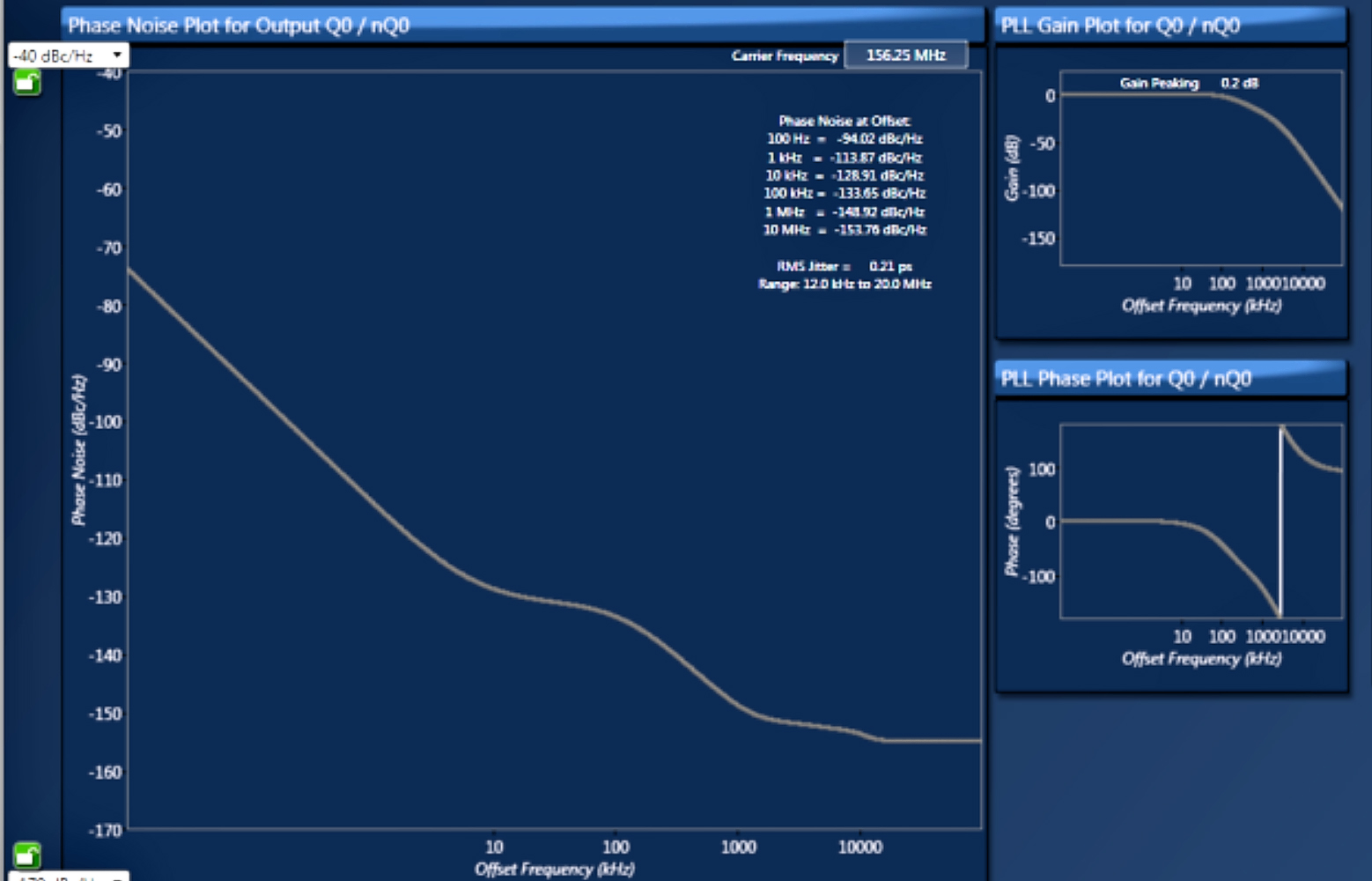
Figure 1: Example phase noise plot from IDT Timing Commander
Integration and the higher power consumption needed to meet low phase-noise targets have changed this into a complex and application-specific effort in terms of ascertaining power consumption and analysing thermal issues. Many recent timing components offer a high degree of flexibility and the ability to power-down unused functions. They also allow the powering of individual circuits at a voltage rail appropriate to the application environment.
In this situation, the solution is a device configurator tool. Not only will such a tool allow designers to determine the settings for the timing device, but a properly constructed one will also provide the designer with power consumption and junction temperature estimates that are valid for that particular board and usage.
Frequency proliferation
Until quite recently, a board designer working in a particular market segment only had to worry about providing five or six different frequencies which were fixed once the board powered-up. For example an Ethernet router might need to provide one of 25, 125 or 156.25MHz for the line interfaces, depending on which pluggable optics module was installed. Today functionality designed for one market space is rapidly being crossed-over to others. That Ethernet router may now need a USB 3.0 port and an SD-card slot for maintenance, requiring 40 and 12MHz clocks. It may also support an Optical Transport Network-compatible uplink port, which could require several of 30-40 different clock frequencies that can change via software configuration. Not only can this result in a lot more frequencies, those frequencies are no longer related to one another by simple integer ratios.
These issues are resolved by timing components that offer increased flexibility and multiple PLLs in a single device. However, flexibility tends to add programming complexity. These new components need to come with a configurator tool, such as IDT’s Timing Commander, which allow a complex device to be setup more easily.
Frequency-domain jitter refers to unexpected, and usually undesired, extra frequencies that exist in all real-world clock signals. These frequency components are especially bad when present on the reference clock for a high-performance Analogue-Digital Converter (ADC) or Digital-Analogue Converter (DAC) since those devices will add many aliases of the unwanted frequencies. Also, physical–layer devices (PHY) for high-speed serial interfaces often include ADCs or DACs internally, so frequency-domain jitter is of increasing concern there too.
In high-performance applications, it is necessary to compare the phase noise performance of the timing component to the input specs on the device it drives. Phase noise performance is dependent on the exact configuration of the timing component and so leading configurator tools will show these plots for each setup.

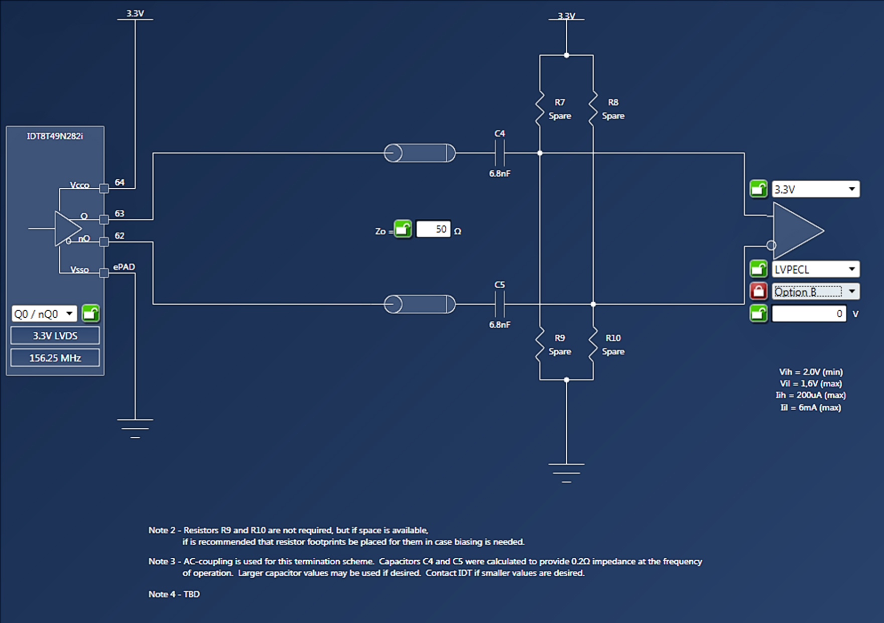
Figure 2: Example Termination Schematic from IDT Timing Commander
The clock tree in a board design is tying together devices from most, if not all, board sub-systems as well as frequency sources like crystals and oscillators. As a result there is often a need to convert signals between single-ended (CMOS) protocols and one or more differential protocols (e.g. LVDS) and often to adjust voltage swings as well. This is usually done with networks of passive components, although active level shifters are sometimes used. For a designer not familiar with the current and voltage specifications of each protocol, this used to require reading through a lot of application notes. Configurator tools will provide recommendations on how to deal with these protocol and/or voltage mismatches on either the input or output of a particular timing component. The same capability can generate recommended schematics and component values for power supply filters and loop filters that may be required, especially on higher-performance devices.
Redundancy and failure scenarios
As connectivity gains increasing importance, reliable operation of everything from mobile handsets to Terabit core routers has become more important than ever. Techniques pioneered for voice telephone switches and fault-tolerant military grade systems have trickled down the network hierarchy. Systems must be designed in a way to minimise likelihood of failure, and the impact if a failure does occur. Many systems also need to meet international standards such as ITU-T G.8261 for their behaviour under failure scenarios.
For timing components this is mainly about switchover and holdover. Switchover is the process of identifying that one clock source has suffered degradation in quality or total loss of signal and switching to a backup source. Holdover is the end-case of switchover and occurs when all backup clock sources are disqualified and there is a fall-back on a local crystal or XO to maintain some level of functionality.
Creating a reliable clock tree is a system-level problem that must be solved at the level of the entire clock tree, especially if an externally-defined, system-level specification must be met. Board designers will need to work with an experienced and system- knowledgeable Applications Engineering team at the timing component supplier to solve these problems today. This is not a problem that can be readily solved on a chip-by-chip basis as those who have tried to mix components from different suppliers can testify.
Designers need an increasingly in-depth level of knowledge of digital, analogue, software, thermal and mechanical design topics. In the area of clocking, this has accelerated rapidly in the last five years with the proliferation of frequencies, tight time and frequency domain jitter requirements and a complex myriad of signal protocols and voltage levels. Leading timing component suppliers have recognised this issue and responded with clock tree builder, parametric search and configurator tools with rich yet user-friendly capabilities. These tools provide valuable assistance to the board designer, but can’t relieve the whole burden. For any issues that remain, there needs to be a knowledgeable applications engineering team that understands the system implications of a clock tree.
Author profile: Ian Dobson, Director of System Architecture, Timing & Synchronization Division, Integrated Device Technologies (IDT), has been with the company for ten years. Prior to joining IDT, Ian spent most of his career in the telecomms industry developing ASIC, board and system-level products. His 25 years of experience include positions as Director of Hardware Development at Alcatel and senior roles at Newbridge Networks Corp and Tundra Semiconductor. He holds a B.A.Sc (Hons) degree from the University of Waterloo in Waterloo, Canada.


