How configurable logic could solve a host of design errors
Configurable ICs delivering multiple logic functions from the same device can save space, reduce logistics and qualification costs.
By Michael Lyons, NXP Semiconductors.
Configurable logic - also known as multi-function logic - is a type of logic that can be configured to deliver one of several different logic functions from the same device. Two such devices can be combined in a single package, resulting in improved flexibility, reduced space, lower system cost, improved inventory management and fewer qualification expenses during development.
Configurable logic is different from programmable logic. With configurable logic, the function is not achieved through programming. Instead, the configuration of input pins connected to either of the supply pins via the PCB layout determines the particular logic function that will be provided. Neither is configurable logic the same as combination logic. Combination logic is one package with two or more functions that can operate on their own or in combination. By contrast, configurable logic is a single package that can be configured to perform nine or more different operations.

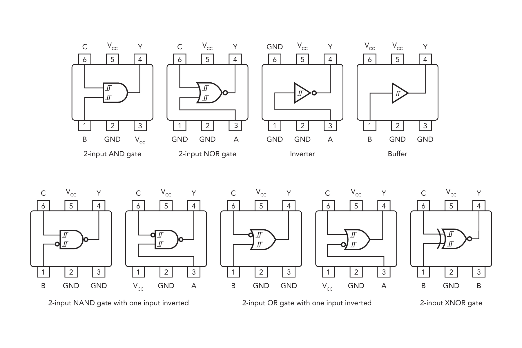
Figure 1
An example of configurable logic is NXP’s 74AUP1G57 which can perform any of several standard functions including AND, NAND, OR, NOR, XNOR, inverter or buffer. It can also perform non-standard combinations, such as a NAND gate with one input inverted. The pin configuration determines which logic function the device performs, so the same device can be used to perform multiple functions in a system. This makes it possible to replace several discrete logic solutions with a single device. The 74AUP1G57 is a single configurable logic gate. Eight patterns of 3-bit input determine the state of each output. All inputs can be connected directly to VCC or GND. Figure 1 shows the different standard and non-standard configurations possible. Non-standard functions, such as a 2-input NAND with one input inverted, combine gates with inverters. This functionality can be achieved in two ways, either with inputs B and C or inputs C and A.

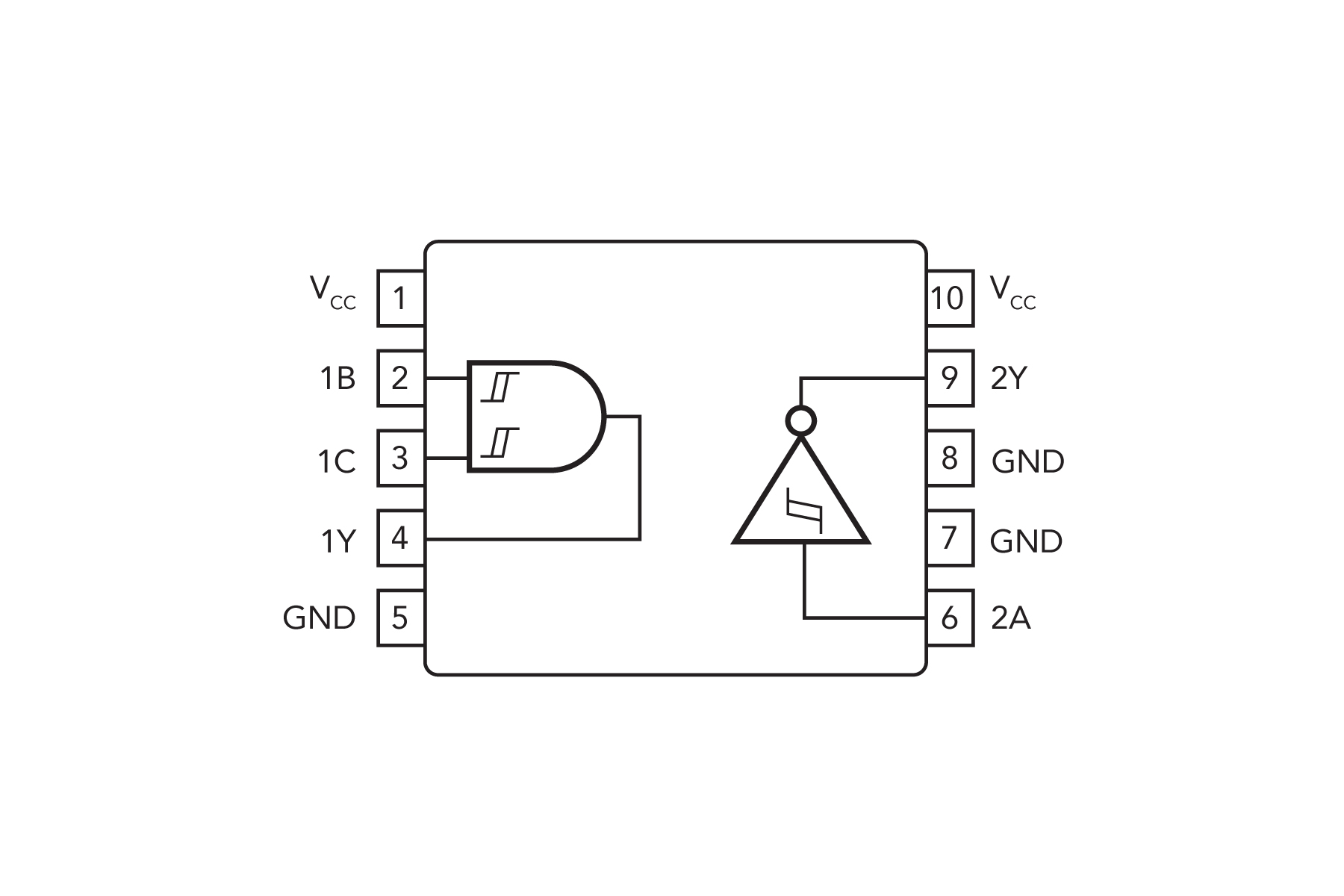
Figure 2
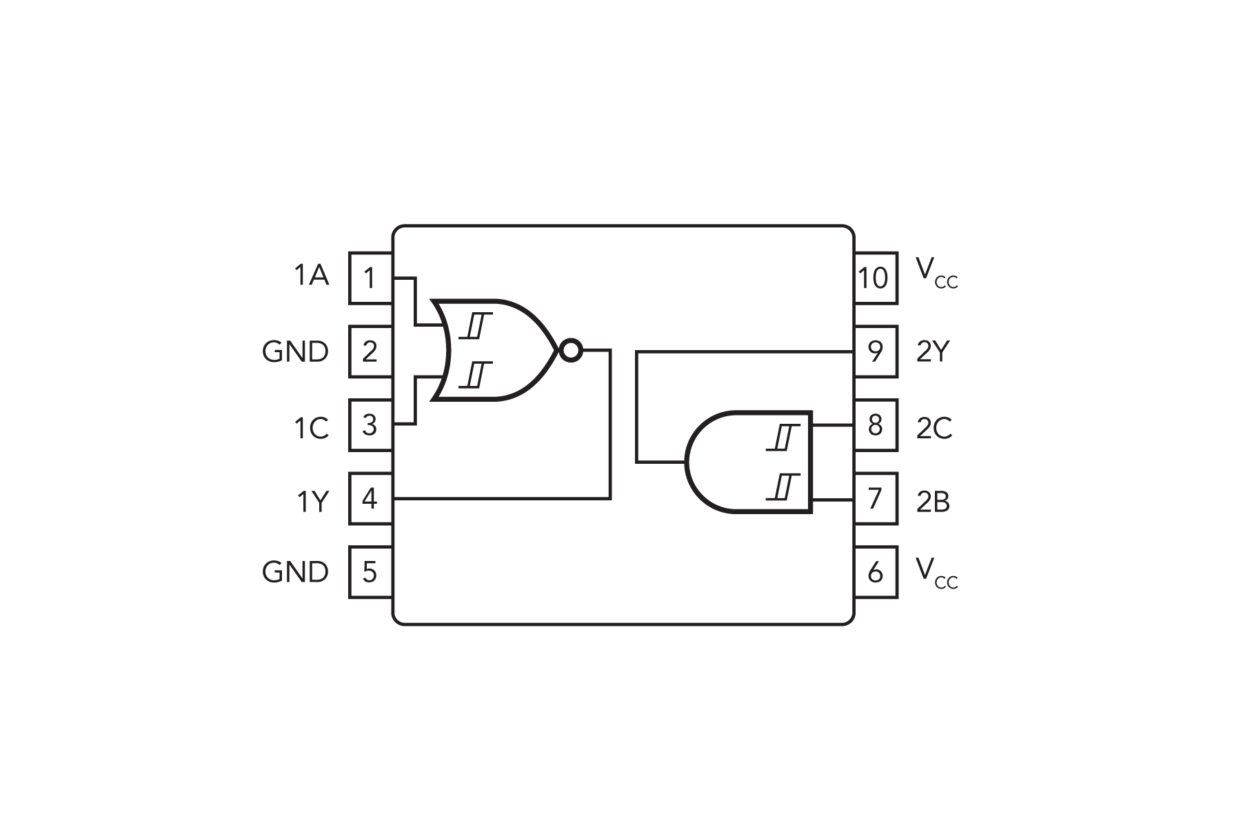
NXP now also offers configurable logic in dual formats. The innovative 74AUP2G57 integrates two 1G57 functions into a single 10-pin package. This integration allows the configuration of many different combinations of logic gates. Figure 2 shows the 74AUP2G57 configured as a 2-input AND gate with a single inverter. (This function is effectively the NXP’s combination logic gate 74AUP2G0804.) Figure 3 shows the 74AUP2G57 configured as a 2-input NOR gate with a 2-input AND gate. (The equivalent in combination logic would be NXP’s 74AUP2G0208.)

Figure 3
Dual configurable logic can be configured to perform the same functions as combination logic, and then some. For example, the 74AUP2G57 is essentially the same as adding 49 combination logic devices to the portfolio. If we include the dual-layout options available with the non-standard functions, the total is equivalent to 81 combination logic products.
All configurable logic products have integrated Schmitt- trigger inputs as standard. Schmitt-trigger inputs have hysteresis built into the switching threshold which allows the interface to slowly changing analogue signals without risk of false triggering or oscillation.
Inventory management
A primary benefit of configurable logic is the number of Boolean functions it represents. In just about any development effort, the inclusion of control logic generally occurs near the end of the project. Only after the key chip set decisions have been made does it become clear which glue-logic functions are required. In the past, to avoid delays in obtaining samples of the correct function, a supply of all standard functions must be maintained. With configurable logic, one device represents several standard and non- standard functions. Therefore, the number of different devices required in stock can be greatly reduced. The same approach can be taken to reduce the total number of items on a bill of materials, simplifying manufacturing logistics. It can also be extended to component qualification: if several functions are all configured from a single device, only one component requires qualification.
Saving power is one of the major concerns facing design engineers today. Designers are also looking to increase performance, by adding features like graphical user interfaces, wireless connectivity, and longer battery life. NXP’s configurable logic is available in the low-voltage CMOS (LVC) family, the advanced ultra-low-power (AUP) family, and in the advanced, extremely low-voltage and power (AXP) family. The LVC family has a wide supply voltage range of 1.65 to 5.5V. It is fully specified at supply nodes of 5.0, 3.3, 2.5, and down to 1.8V. For power-sensitive applications, the AUP family has a supply range of 1.1 to 3.6V. It is fully specified at supply nodes of 3.3, 2.5, 1.8, 1.5 and down to 1.2V. For further power savings, the AXP family has a supply range of 0.7 to 2.75V. It is fully specified at supply nodes of 2.5, 1.8, 1.5, 1.2, and down to 0.8V.
Single-gate AUP and AXP configurable logic have a maximum static current dissipation of 0.9 μA and 0.6 μA respectively. They have dynamic power-dissipation performance (CPD), of 3.1 and 2.9pF respectively. These ratings show that AUP and AXP are the lowest-power logic solutions in the industry.
Advanced packaging
Another concern is reduced footprint, especially for mobile and portable designs. Configurable logic is available in a 10-pin TSSOP package, as well as in smaller footprint, leadless 10-pin XSON and XQFN packages. The XSON10 represents an 89% footprint reduction compared to the leaded TSSOP10. This footprint reduction increases flexibility in space-constrained layouts. It also allows the use of smaller PCBs and the potential cost reductions they enable.
By realising multiple functions within a single package, configurable logic increases design flexibility, reduces inventory cost, and enables faster qualification in end-user applications. Now, with NXP’s new dual PCB configurable logic devices - single-package solutions each containing two configurable logic devices - engineers have an even greater degree of freedom when it comes to finding a low-cost way to use glue logic in a design.
NXP and Mouser launch Big I.D.E.A. design contest combining multiple NXP Business Units and products
The Dual PCB Configurable Logic product line is the centrepiece in a design contest featuring products from NXP Business Units, including Logic, Smart Analog, Load Switches, Protection and Filtering, Small Signal MOSFETS, Small Signal Diodes and more. The Dual PCB Configurable Logic Contest will be this year’s entry in the 2015 Big I.D.E.A. (International Design Engineering Award) sponsored by NXP and Mouser. The contest launched worldwide in January 2015 with huge cash and merchandise awards for the most creative design using all the NXP products together in one application solution. The contest entails engineers navigating from the sign-up process, through an on-line schematic tool, to working with a demo board in the final submission. Prizes are awarded at every stage of the contest, so more engineers can qualify, regardless of how far they progress in the contest.


