Integration boosts performance & functionality, not power
How to boost performance and add functionality to portable medical devices without affecting the power budget. By Franco Contadini, Principal Field Applications Engineer, Maxim Integrated.
A significant percentage of the worldwide adult population needs to monitor personal vital signs (i.e. blood glucose level, blood pressure, oxygen saturation level) regularly. Not surprisingly, we are seeing more and more requests for portable medical devices that perform these tasks and even integrate more functions. This trend will not stop.
Space, weight, reliability, security, and power consumption are the key elements for designing modern portable medical devices. A typical portable medical device today usually requires several macro blocks: battery management to handle the power source, either a primary or rechargeable battery; an AFE to condition and convert the signal coming from the sensor into a digital word; and a MCU to perform mathematical calculations on the acquired signal, display that information on an integrated LCD or transmit the data to a wired/wireless device. Typically different discrete devices are used to provide all these functions.

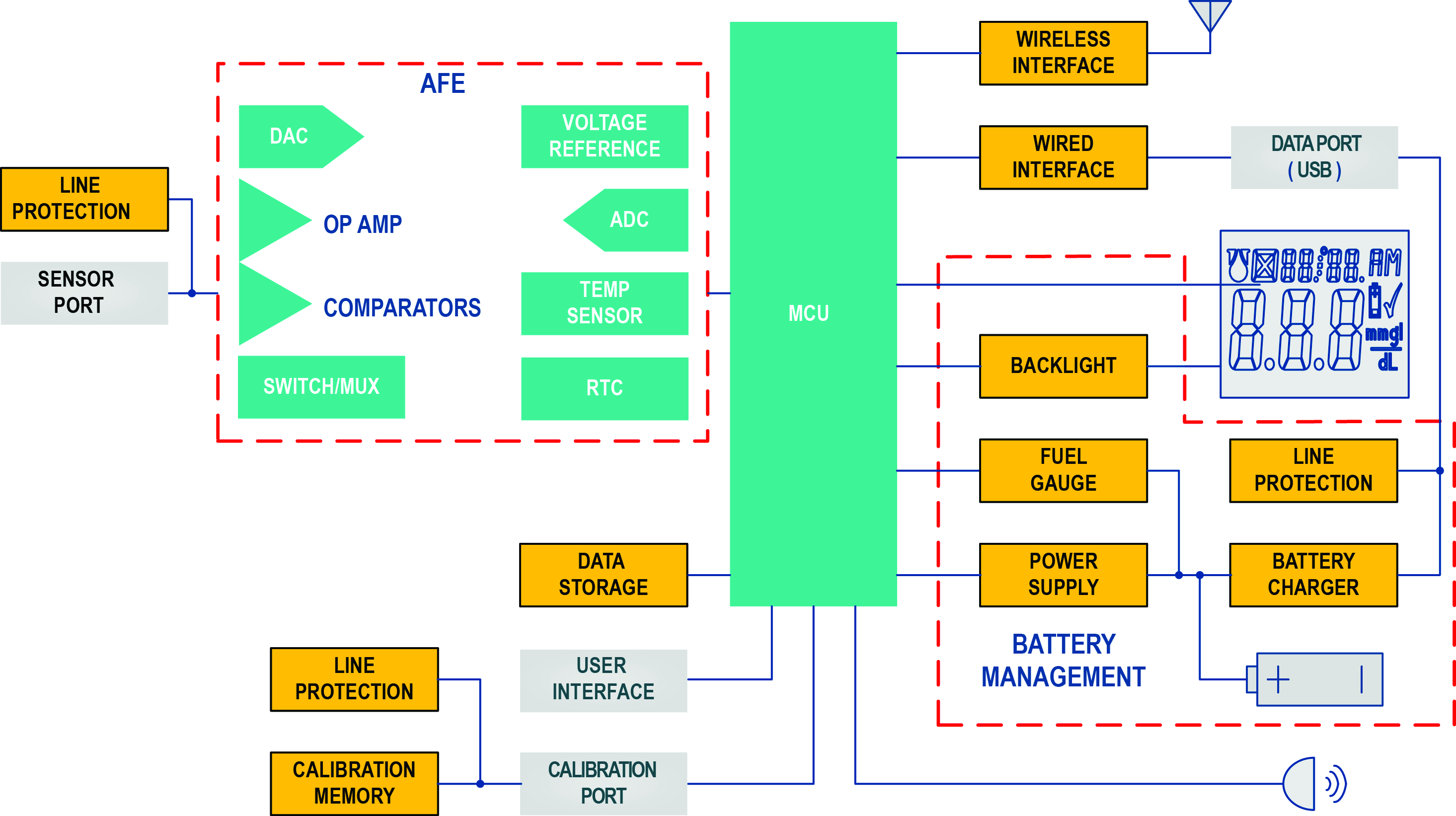
Figure 1 - Block diagram of a basic power solution with multiple discrete components for a portable medical device
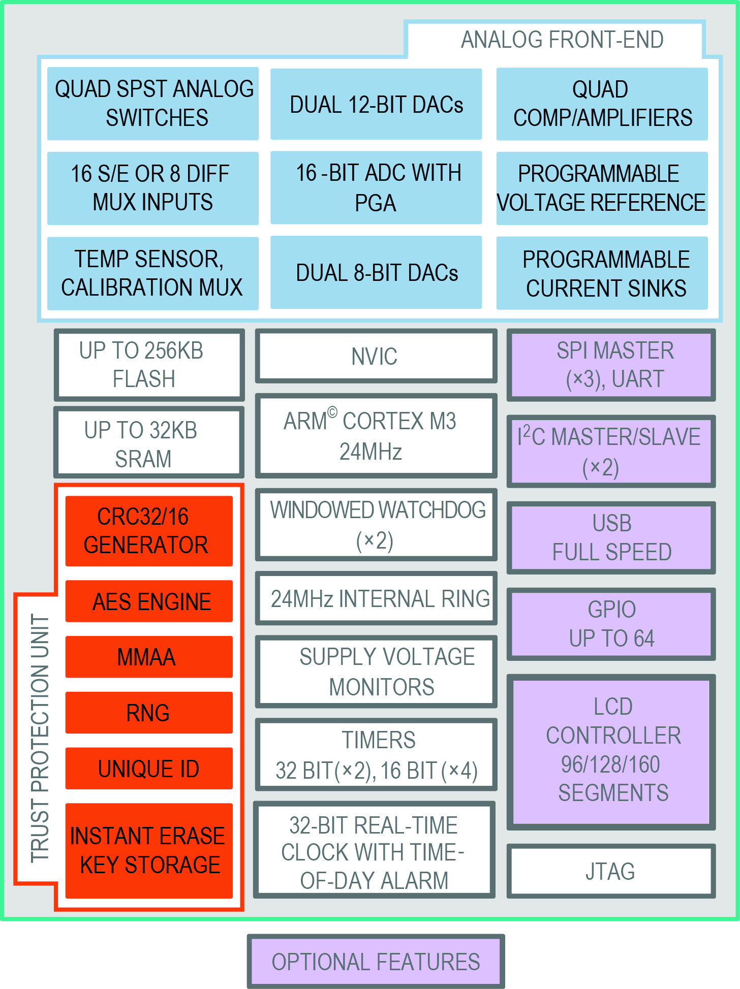
A typical functional block diagram for a discrete power solution is shown in Figure 1. The battery-management block consists of the battery isolator, battery charger, fuel gauge, backlight supply, and linear/switching regulator. The AFE usually requires an ADC, DAC, op amps, comparators, analogue switches and voltage reference. This use of so many discrete devices can potentially impact system reliability, while they definitely increase cost and add board space. Now, dual-chip integrated solution comprised of a MCU SoC and a PMIC is available that boosts overall device performance; the MAX32600 MCU SoC (Figure 2), based on an ARM Cortex M3 core, is differentiated by its high-performance AFE and integrated, advanced security for trust protection. A wired and wireless communication interface gives the user multiple choices to connect the medical device to another portable host like a PDA or smartphone.

Figure 2 - This highly integrated MCU SoC is optimised for portable medical devices. It features an AFE and high security in a Trust Protection Unit. Wired peripherals augment system flexibility and multiple power-management modes save power
The analogue domain
The AFE consists of a SAR ADC at its core. The ADC’s high 500kS/s rate and the 16-bit resolution let the MCU increase resolution using oversampling and averaging, if the bandwidth of the input signal is limited. Oversampling and averaging, in fact, increase the SNR, thereby gaining additional bits of resolution.
The ADC can be configured to collect bursts of data at a regular interval, provide Direct Memory Access (DMA) for the data to SRAM and then wake up the processor. The ADC’s interface provides a programmable burst sample rate and a programmable burst length for averaging (2, 4, 8, 16, 32, 64, 128). The input signal is selected through a configurable, single-ended/differential multiplexer. In front of the ADC is a differential amplifier with a programmable gain of 1, 2, and 4. A reference voltage programmable at 1.0, 1.5, 2.0, and 2.5V maximises the dynamic range. Four uncommitted op amps with comparator mode and four SPST switches can be used for additional signal conditioning.
Two 12-bit DACs, two 8-bit DACs, an additional voltage reference (also programmable, as the previous one), a temperature sensor that can use an internal or external PN junction, and programmable current sinks for driving LEDs complete the analogue design. An interpolation filter (1:2, 1:4, and 1:8) is available on the 12-bit DACs and 8-bit DACs to improve dynamic performance and reduce bus bandwidth.
It is possible to synchronise the start of the DAC pattern with ADC sampling. This enables easy impedance measuring using digital waveform synthesis and synchronises circuits for coherent waveform generation and ADC data collection (Figure 3).

Figure 3 - Signal-processing block diagram for impedance measurement
Embedded security is essential to protect the integrity of the data generated by the medical device. This SoC firmware is protected, because the flash and SRAM can be encrypted using a key stored in an internal battery-backed memory. Device authentication is provided through embedded crypto blocks and is suitable for both symmetric and asymmetric schemes.
Low power integration
The SoC operates with a voltage down to 2.2V, a major benefit for a portable medical device powered from a primary battery. The embedded core has a 175µA/MHz operating current at 24MHz, a 1.8µA low-power mode with a RTC enabled and multiple power-management modes to save power. The option to shutdown inactive peripherals saves even more power. A six-channel DMA controller enables peripheral operation while the MCU is in sleep mode. In this way the ADC can be programmed to scan input channels, collect data and wake up the core only when processing is needed.
Embedded peripherals provide all the functions needed to implement a portable medical device.; a USB 2.0 full-speed controller with PHY allows direct connection to the USB cable. This design reduces board space and overall system cost. An integrated voltage regulator enables smart switching between the main supply and VBUS when connected to a USB host.; a feature that is especially beneficial in systems where the VDD power supply is a battery.
Up to three SPI master UARTs enable synchronous communication with multiple peripheral slave devices. Data transfer is possible up to 24MHz. DMA is supported for both the transmit and receive buffer. The two I2C bus master/slave interfaces permit communication with a wide variety of other I2C-enabled peripherals. Both the master and slave protocols are supported. Two USART ports support either full-duplex asynchronous or half-duplex synchronous communications.

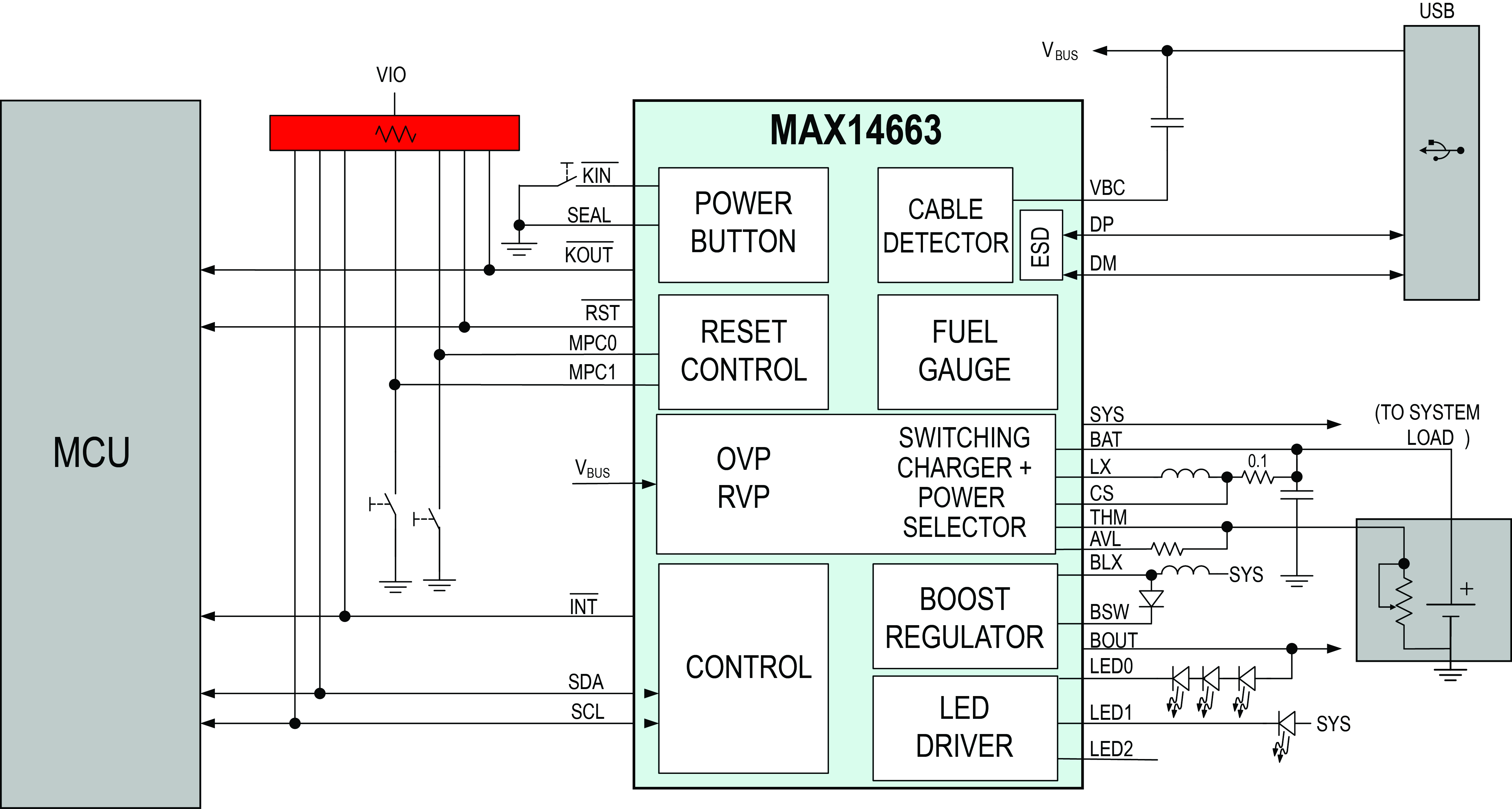
Figure 4 - BGM-optimised power solution with cable detection
The MAX14663 PMIC (Figure 4) integrates a Li+ switching charger and is an optimised power solution for space-constrained portable medical devices. Used with the MAX32600 MCU SoC, it will maximise power, and ave valuable design space. Portable medical equipment must retain a reliable charge and be available for use at any moment, consequently the design focus is on preserving the charge during the device’s ‘shelf life’. The MAX14663 integrates a switch to turn the battery off and keep it disconnected until the medical device is turned on for the first time by the end-user. For example, at the end of production phase an I2C command or a proper connection of the SEAL pin can be used to disconnect the battery, thereby preserving the charge during device’s shelf life.
An integrated fuel gauge, based on ModelGauge technology, uses only voltage information to provide a State Of Charge (SOC) for the battery. Using a very detailed, nonlinear model of the battery, it accurately monitors the charge and battery behaviour. The battery model, provided by Maxim following a characterisation in its factory, has to be loaded in the device’s internal volatile memory for proper operation.
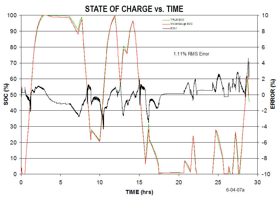
Figure 5 illustrates the performance of ModelGauge technology. Random load sessions and charge sessions for random amounts of time show the battery SOC rising and falling. The green line is the reference SOC and red line is what ModelGauge reported as the SOC. It can be seen that the green line is very difficult to distinguish from the red line. In fact, the lines are almost identical. The difference between these two curves appears in black on the right Y Error axis. These data show that the ModelGauge fuel gauge acts like a healing mechanism in the error, moving error up and down around 0%, rather than an accumulating mechanism like a coulomb counter.

Figure 5 - SOC vs. time. Data show that ModelGauge technology does not accumulate error over time
Fuel gauge active current is 23µA. This fuel gauge automatically goes into a 4µA hibernate mode when the charge/discharge rate is low. This background mode does not compromise fuel-gauge accuracy. Alerts can be used to reduce the system power by allowing the system to completely shut down, even shut down some oscillators, and to reach this 4µA background mode. The fuel gauge uses an alert to wake everything up.
A switch-mode battery charger minimises power dissipation. During charging, this function prevents PCB hot spots that can compromise accuracy when small signals, sensitive to temperature variation, have to be measured. Current is regulated using operating modes: when the battery voltage is less than the prequalified threshold voltage (programmable via I2C from 2.4 to 3.1V), current is limited to less than 0.1C; in Fast-charge mode, CC/CV mode current is regulated according to the programmed fast-charge current. The range is from 50 to 500mA in 25mA steps; if autostop mode is selected the charge will be terminated when the programmed constant voltage (from 3.5 to 4.4V) is reached and the current has dropped to the programmed value from 12.5 to 150mA. The charger can also be stopped using an I2C command.
The charger also monitors battery temperature through a battery thermistor. Temperature information can be used to implement a JEITA (Japan Electronics and Information Technology Industries Association) recommendation where, for safety, the termination voltage and fast charge current are modified according to the battery’s temperature.
Increasing battery life
Voltage provided to the system comes from USB when VB is within an acceptable range, and from the battery when VB is not present. This operation occurs automatically. An inductor-based boost converter can generate the high voltage needed for an OLED display or a white-LED string used for LCD backlight. The output voltage is adjustable via I2C from 6 to 17V in 1V steps. A true-shutdown switch disconnects the load completely to minimise current consumption.
Three independent, linear current regulators can be connected directly to the voltage generated from the boost converter. Now the current can be regulated up to 32.5mA in 25 steps. A PWM signal can be used for dimming. The system is protected against a reverse voltage up to -5.5V applied to VBUS, and is protected against an overvoltage up to 28V. This protection prevents any fake battery charger that tries to use the USB interface to damage the equipment. The system voltage is regulated to 5V; it is regulated for a VBUS voltage up to 6.6V. If the VBUS voltage rises above these thresholds, the system voltage is automatically disconnected to protect the equipment.
ESD protection of ±15kV is provided on the VB, DP, and DM pins. Another feature implemented on the USB side is cable detection. The system will detect a cable presence when the upstream port is OFF and, therefore, when VBUS is not present or when the cable is connected on the device side only.
Detection is accomplished by injecting a small current when VBUS is not present, and measuring the cable capacitance and capacitor connected to the upstream port. The threshold used for detection can be programmed via I2C to accommodate different PCB layouts and connector type.
Efficient power management for modern portable medical devices can be implemented without major architectural changes; beyond the obvious benefits of smaller and cheaper solutions, fewer discrete devices means a more reliable solution to the ultimate benefit of everyone.


