How to tackle leakage current in the automotive industry
In today’s automotive industry there has been a gradual shift from traditional concerns like area and cost to power consumption and leakage current. Consequently, the designers focus more on techniques like clock gating, power gating, dynamic voltage and frequency scaling to meet the requirement.
Authors: Deepak Mahajan, Saloni Raina, Abhinav Nawal, Freescale Semiconductor
This lead to the introduction of various advanced low power modes in present day SoCs (Silicon on Chip) where the user has tremendous configurability on enablement of clocks, peripherals and power domains. We as the product owners have the responsibility to ensure that any configuration that we claim to support, should work seamlessly, even if the possible configuration count touches as high as a million. Even a single failing configuration out of the million possible ones makes us liable to the customer. A recent research shows that clocking and power defects are the top contenders for causing Re-spins (product revisions).

Figure 1
This calls for a need to have a well defined low power verification/validation plan wherein all possible scenarios are well thought of and tested before the chip reaches the customer. In this article we intend to highlight some scenarios which are a 'must have' from low power testing perspective. In the following section we are listing down critical checks that should be done for having complete verification coverage of low power architecture.
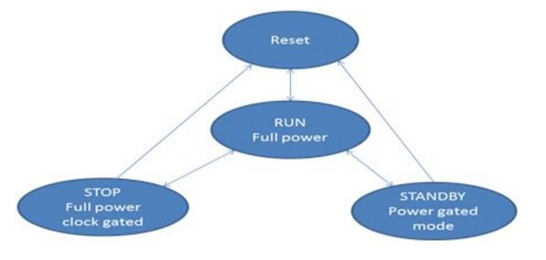
Figure 2. Basic mode transitions diagram showing 4 basic power modes.
Mode transition patterns while running in digital simulations can check only the basic entry exit sequence but this alone is not enough. There are many other things that need to be checked in low power modes, a glimpse of which is a part of the coming section. Simulations can check the digital signals that are the part of low power protocol like assertion of isolations, opening of switches, supplies, but what is missed is the exact design behavior, as digital simulations at RTL level cannot mimic the exact power gating sequences. Even though Analog and mixed simulation is a solution to the above problem, where design actually takes the supplies into account to generate the output but since AMS simulations are very slow and setup is quite complex, each and every scenario can’t be touched upon with this approach. What is needed is a Low power simulation tool that can be used to simulate the power gated scenarios at RTL itself. In the industry there are many such tools available, one of them being 'Common Power Format (CPF)'.
CPF file is input to simulator on basis of which it injects ‘x’ on the logic which is power gated. This x injection adds a lot of pessimism leading which non-resettable flops and wrong reset/clock issues can be found. But this tool alone can’t do wonders! Along with the tool is required a set of intelligently developed patterns with an intention of complete scenario coverage. CPF file contains information on the power domains and digital signals like switches that can be used as shutoff conditions for power gating.
Also power aware GLS simulations are run to check for any issue introduced during Backend cycle (Placement and routing). Power aware gate level simulations are also known to unhide all the x-optimism issues due to incorrect RTL behavioral coding.
Below is the brief description of the categorised checks that should be run with power aware RTL and Gate level setup. Detailed explanation of these is not in scope of this article.
1- Mode transitions
- All mode transitions with coverage monitors
Apart from the clock gating options, SoCs also have multiple power domains which can be selectively powered up/powered down according to the application requirement. It is very important to test transition from every mode to every valid low power mode (clock gating or power gating). Also, having a quantitative measurement of what all modes transitions have been covered is important. This can be done by having coverage monitors. - System clock coverage in low power modes
There is an option of enabling/disabling clocks in the target low power mode. Also, the clocks in the current full power mode are configurable. It is important to have a coverage matrix to check mode transitions from full power modes to low power modes (and exit from it) with all possible clock combinations. - Low power entry/exit protocol checks
- Wakeup from low power
There are multiple sources (internal and external) that can bring the SoC out of low power mode. Ranging from every interrupt source for clock gating condition, to a few selected wakeup sources for power gating case, requirement is to test every possible low power recovery source exhaustively.- Test every valid reset/external wakeup/internal wakeup source.
- Test the above sources with changing clock configurations, with no clock condition being a critical test.
- Frequency ratios of the wakeup source and the logic which is latching that wakeup should be checked in exhaustive manner to rule out any pulse miss sort of thing.
2- Reset connectivity
- Power domain reset connectivity check
Modules that are powered down during a low power mode should always be restored to their reset values on low power exit. While modules that are powered up throughout this low power entry/exit sequence are supposed to retain their existing configurations. This is a very basic but yet a very important test where there are high chances of incorrect power domain reset connectivity.
3- Expose checks in low power
- Clock expose check
There is a provision to bring out system clock and other available clocks to pad such that they can be used for debug purposes after silicon arrival. All such clock sources should be checked in every possible low power mode. All available clock dividers should also be covered under this test. - Signal expose check
Similar to clock expose, we have certain system level signals coming on to the pad for debug purposes. Checking this connectivity is what comprises the signal expose check.
4- IP features checks in low power
Testing the control signals (like pull up enable, pull down enable, pull up select, slew rate enable) of pads is very critical, as incorrect functioning of this pad state control feature may cause unwanted leakage current in low power modes. Also checks should be done to ensure that pads which are in always ON domain should retain their states in low power modes as per requirements.
- Module enable/disable check
If there is a possibility to selectively disable a module in low power, it is important to check if it actually behaves as configured. This can be tested by enabling the module in full power mode, while keeping it disabled in low power modes. In full power mode itself, configure it to perform some function and generate interrupt when the function is completed. Give a low power entry in the meanwhile, SoC should remain in low power. While repeat the same process by enabling the module in low power, SoC should come out of low power due to the interrupt generated by the module. - Register access in low power
In advanced low power modes, some power domains are switched off while the others still keep functioning thereby reducing the power consumption. The entire memory map that is supposed to be powered up should be accessed to check for any discrepancies. This is a basic check to check that the clocks and resets to all IP’s in ON domain is correct. - Pin muxing check
Though all available pin muxing options are tested in full powered modes, it is important to test them in low power modes as well, to discard the possibility of issues creeping in due to the various processes that are a part of low power transition of the SoC. Also there can be some isolations in path that come into picture in low power modes and cause issues while interactions with GPIO’s. - Cores and interrupt routing
Enabling/disabling cores in low power modes may/may not be configurable. It is important to test if the cores are functioning as per design, in low power modes, and the interrupts are routed to the right core for servicing and core is able to service the interrupt properly in low power mode. - System fault detection and correction in low power
Every SoC has an error detection unit which is also responsible for system recovery in conditions of fault occurrence. This unit should be functional in low power modes as well. Test should be conducted by introducing fake faults and check if corrective actions are taken. Also, the SoC should be able to exit from low power after recovering from the fault. - Pad control check
- Seamless operation of IP’s across mode transitions
If a module can operate in both run mode as well as low power modes, it is possible that a low power request is initiated when the IP is still performing some function. For example: CAN, DSPI, LINFLEX or DMA transactions. Some modules may support seamless operation through low power entry, while others may not. It is important to test and document clearly the expectation in such a scenario. - Debug features of IP’s to be check in low power
- Having a fully functional debug interface in low power modes if important and testing it is even more important from customer perspective.
5- Physical checks in low power
- Low power RAM retention
Typically a portion of the RAM can be retained during low power modes. This is a requirement for booting purposes after low power exit, especially for devices with no flash memory. In this case negative checking is also a must to do. All memory portions that are configured to be off in low power modes should be off so as to avoid any extra leakage in that mode. Add a proper check on the switches that controls the supply to RAM.
Test this feature in the following two conditions:- Clock to power controller ON in low power mode
- Clock to power controller OFF in low power mode
- Clock OFF case is more pessimistic, as it can find cases where there is race condition between the power controller state machine and clock gating state machine. It can happen that the clocks are gating off first and till that time the power controller has not turned off the supplies to memories and other IP’s. This may lead to issue like 'memory is always retained' causing extra leakage.
- Run the sanity patterns across PVT (Process Voltage Temperature) conditions to check if the chip is meeting the datasheet specifications.
- Soak testing
Testing the system in low power modes extended over significant period of time at-least overnight to discover how the system behaves under sustained use. - Current measurements in low power modes
6- Corner case checks
Apart from the exhaustive feature and connectivity checks, it is important to stress the system to uncover the corner case scenarios, if any, existent in the system. These include:
- Multiple resets (different sources) occurring back to back.
- Random abort time while entering into low power
- Sweeping loss of clockthrough low power modes
Even though this may seem too big a plan to cover during SoC Verification/Validation phase, but as highlighted earlier, these are the 'must haves' of any low power test plan and should anyhow be covered depending upon what your SoC supports. What is required is a well defined unified test plan for pre-Si SOC verification/validation and post-Si validation such that every test is covered at least in one of the three phases. This would help reduce redundancy and lead to faster execution while avoiding any coverage gap.
This article gives a brief overview of all the conditions to be tested for Low Power. Details of these tests and ways on how they can be automated will be followed in the series of articles where the individual testing would be taken up in detail.


