Fan-out wafer level packaging is entering a new era
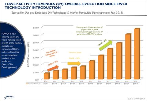
Fan-out wafer level packaging is now entering a new era. With a high expected growth of the market, multiple new companies, OSATs and even foundries are involved in this platform. According to Yole Développement’s Fan-Out and Embedded Die: Technologies & Market Trends and Equipment & Materials for 3DIC & Wafer-Level Packaging Applications reports, the market reached more than $150m in 2014 and a CAGR of 30% for the next 5 years is expected, driven by mobile applications and the need of very thin packages for high I/O devices.
Yole recently had the opportunity to interview David Butler, Vice President of Product Management and Marketing at SPTS, the semiconductor device division within Orbotech. Butler has shared his point of view on fan-out wafer level packaging platform with Yole’s analysts.
Yole Développement: Fan-out, as an emerging packaging platform has certainly raised a lot of interest in the industry. Investments in equipment and other necessary infrastructure to support fan-out technology have been made and fan-out has already been successfully adopted in production. We continue to see a high interest in this platform and we are expecting a high growth for the next few years, therefore, further equipment needs and investments. Can you please confirm and comment on the industry’s preparation for the next wave of growth in fan-out? Have you seen increasing equipment spending in the past year, and do you believe it will continue to further increase this year as well?
David Butler: In the last 12 months, FOWLP has emerged from a relatively small base to become one of the most active topics in the packaging world. It started with eWLB, the Infineon designed platform that was licensed to a small number of companies at the end of the last decade, notably STATS ChipPAC and NANIUM. Those two companies now lead the FOWLP market. During 2014, more companies announced their own FOWLP platforms, including Amkor with SLIM, SPIL with SLIT, Intel EMIB and perhaps the most vocal, TSMC with InFO. We are aware of additional companies that have plans in that direction but have not yet gone public. These new announcements have coincided with a ramp in equipment spending, from which SPTS has benefitted. One major OSAT told me that of all their projects that come under the heading of ‘Advanced Packaging’, their FOWLP project had received by far the most interest from their customers, backed up with considerable urgency. The need is real and immediate.
Yole Développement: What are the main devices that will drive this next growth?
David Butler: Mobile devices and tablets for high bandwidth applications. Baseband processors, RF transceivers and power management IC’s are being embedded in these mold wafers. NANIUM speak of the advantages of being able to mount RF devices in close proximity to multiple passives, delivering data transfers of more than 60GHz. Line and space reductions will move FOWLP into the reach of even higher performance parts such as memory and application processors.
Yole Développement: What are the requirements and challenges coming from fan-out manufacturers regarding equipment, in terms of warpage, cost and precision? What are the critical steps in the process? How is SPTS handling these demands and what is your roadmap?
David Butler: Warpage is a significant challenge. The epoxy mold wafers can be warped after curing, and the size and shape of the warpage can change for different shapes and density of the embedded die. In an effort to reduce cost and package height, the thickness of the substrate reduces as well, although this tends to make the wafer less stiff and therefore flatten under gravity. We have applied significant resource to develop hardware that can handle wafers up to 6mm bow, and processes that minimise temperature induced shape shift. I do not expect the industry to move to much more than 6mm bow, since it is by no means simple to produce uniformly thick conductors on a substrate showing that amount of warpage. Another challenge is contamination. The mold contains moisture and other gases which will contaminate the metal pad unless managed correctly. As an added complication, these wafers cannot tolerate high temperatures, so the PVD equipment supplier cannot do a simple 400°C degas as it would in the front-end of the fab. The chart below shows the effect of degas time on contact resistance; it can take up to 35 minutes to get a clean metal-to-metal contact when embedded in epoxy mold. In practical terms, using a single wafer degas on a PVD system will result in a throughput of much less than 5w/h, which will not satisfy this market.

The full interview is available on I-Micronews.


