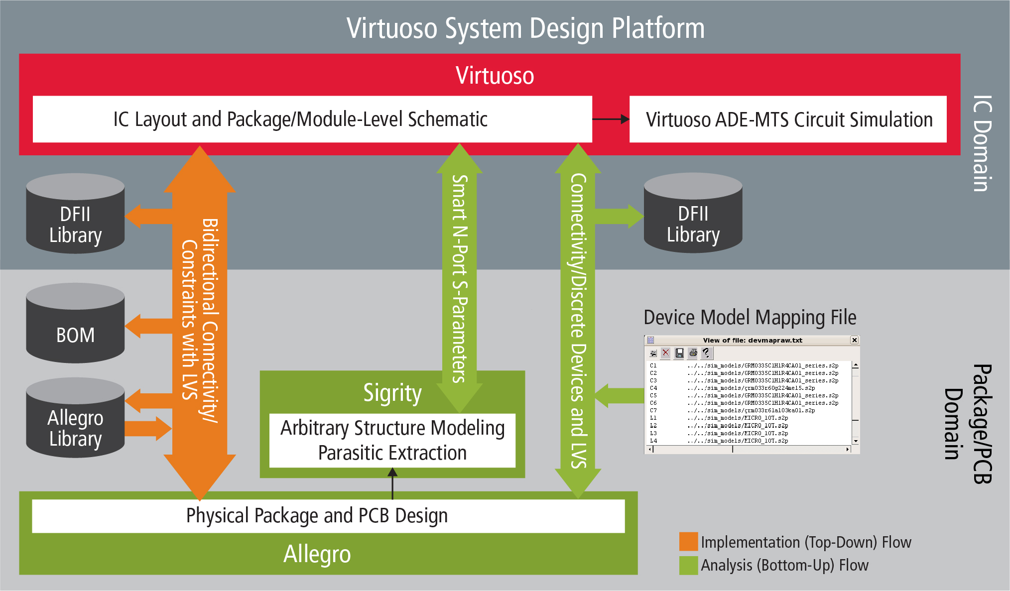
Design platform improves productivity and cycle time
A formal, streamlined and automated co-design and verification flow between the Cadence Virtuoso platform and Allegro and Sigrity technologies has been announced by Cadence Design Systems, the Cadence Virtuoso System Design Platform. This higher level of integration enables engineers to design concurrently across the chip, package and board.
By automating what has until now been a manual process, the Virtuoso System Design Platform minimises errors and can reduce layout versus schematic (LVS) time between IC and package from days to minutes.
Until now, advances in silicon technology have been sufficient for continued improvement in microelectronics products. Given the complexity of today’s chips, packages and boards, ICs based on both silicon and non-silicon materials are now required to design optimal high-performance systems. As a result, this trend is driving the need for engineers to integrate multiple heterogeneous technologies in a single product, affecting the performance and functionality of ICs and introducing a new set of challenges for semiconductor companies. To address these challenges, Cadence has developed a novel, cross-platform solution that streamlines and automates the design of a package or module featuring off-chip devices and multiple ICs based on differing process design kits (PDKs).
The Virtuoso System Design Platform allows IC designers to easily include system-level layout parasitics in the IC verification flow, enabling time savings by combining package/board layout connectivity data with the IC layout parasitic electrical model. The resulting automatically generated 'system-aware' schematic can then be easily used to create a testbench for final circuit-level simulation. Until now, designers were only able to make changes after time-consuming manual checks involving spreadsheets and other ad hoc/manual methods, which can take days. By automating this entire flow, the Virtuoso System Design Platform eliminates the highly manual and error-prone process of integrating system-level layout parasitic models back into the IC designer’s flow, reducing days of work to mere minutes.

“We had been looking for a solution that created a tighter level of integration between our Virtuoso IC designers and our Allegro package design team,” said Toshihiko Himeno, Group Manager of the Design Methodology & Infrastructure Group at Toshiba Memory. “The new Cadence Virtuoso System Design Platform enables us to design a single hierarchical schematic to drive both IC and package layout while providing LVS checking, along with automating the library development process. We believe this new streamlined methodology will help to reduce our design-time cycles. Not only does the Virtuoso System Design Platform save us valuable time, but it eliminates what had until now been an error-prone process, giving us confidence that we’re taping out an accurate design.”
“With the increasing complexity of today’s chips, packages and boards, designing each in isolation is no longer feasible,” said Tom Beckley, Senior Vice President and General Manager of the Custom IC & PCB Group at Cadence. “Cadence’s holistic, end-product focus from chips to packages to boards enables our customers to deliver the best possible systems and devices. With the Virtuoso System Design Platform, our customers can reduce risk and get to market faster with optimised designs featuring multiple heterogeneous ICs, including RF, analogue and digital devices. This innovation is yet another result of Cadence’s System Design Enablement strategy.”


