A class of their own
Incorporating power and intelligence can satisfy the stringent requests of the automotive market when using Class D audio power amplifiers. By Edoardo Botti, Design Architect Princ. Eng. II with STMicroelectronics, and Marco Gaeta, Technical Marketing Manager at ST.
Audio amplifiers in car radios are becoming more than ‘simple’ power amplifiers. The OEM market, where car radios and sound systems are sold together with the car, is extremely demanding.
In addition to the classic features like output power, distortion, noise, cross talk, frequency response, damping factor and so on, the modern audio amplifier for automotive must perform many other functions and fulfil unusual specifications; unusual, that is, for current audio amplifiers.
It should come as no surprise that in the automotive market there is a trend for the drastic reduction in power dissipation, to reduce power consumption, size, and weight of the heatsink. In audio amplifiers, this requires a change from the standard Class AB technique, to SB/SBI, and then to higher efficiency systems like the Class D.
Sophisticated diagnostics are now also required, to inform the system microprocessor about all the working conditions of the device like temperature, clipping, overload, shorted outputs, shorted and open load for woofer and tweeter.
Furthermore, a car’s unique environment means noise produced by digital circuits wreaks havoc with ‘sensitive’ analog lines. Moreover, the system must conform to the extremely severe EMI rules, both for emission and immunity, required by this environment.
The answers to all these issues can be addressed systematically by using a new monolithic approach comprising the followings key characteristics: digital input signal (I2S or TDM); digital signal processing, and; Class D (or PWM) power amplifier with output filter inside the feedback loop.
In order to have all of this in a monolithic device, a suitable technology must be able to incorporate analog circuits together with high density digital circuits and efficient power MOS transistors. This technology is called BCD, (Bipolar, CMOS, DMOS).
A multi-die approach in a single package (stacked or side by side) can limit features because of the large number of interactions needed between the digital part and the analog parts of the device that are not feasible with bonding connections.
DSP powered
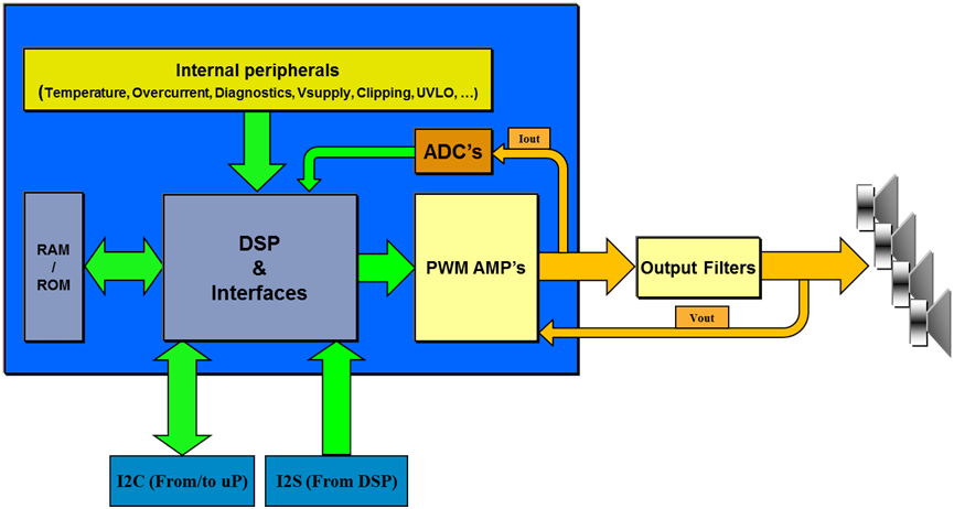
Figure1 shows the block diagram of a typical ST class D power amplifier; the DSP block is the core of the device. As a digital circuit able to process the signals coming from the outside world, it manages I2C bus, the turn-on sequence and the diagnostics. This block also produces the audio signal to drive the PWM amplifier and the information regarding the output current through the ADCs.

Figure 1: Block diagram of a typical ST Class D power amplifier
The PWM AMP’s block receives the input coded by the DSP and produces a PWM output able to drive the loudspeaker. The output is in bridge configuration (balanced). The PWM frequency is defined by the I2S clock frequency and by the programming. An LC filter that removes the PWM carrier, typically at 352.8kHz with input sample rate equal to 44.1kHz, is located between the device and the loudspeaker.
A loop goes back to the DSP after analog to digital conversion with a signal equivalent to the output current. This signal is used for diagnostics and protection purposes.
An analog feedback loop is also present. It is important to notice that the feedback is taken after the ‘Output Filter’ block. This technique assures important advantages when compared to the standard feedback loop used in common PWM amplifiers, where the Output Filter is outside the feedback loop, or in systems without any feedback loop.
Market challenges
All the inputs to the power amplifier are digital. This means an extremely high robustness against disrupts present on the board. Additionally, the high interference immunity of the digital inputs meets all the requirements regarding susceptibility to electromagnetic fields generated by broadcasting stations and cellular phones.
It is important to provide outstanding performance in frequency linearity, damping factor and electromagnetic radiation reduction. The analog feedback, including the output filter, benefits the power amplifier with the following features:
- Precise output voltage versus the digital input signal, independent from the power supply,
- THD almost independent from the output filter non-idealities means that an inexpensive and low performance filter can be used,
- The frequency response is largely independent of the variation of the load characteristics, allowing the same application to be used to drive different loads,
- Excellent damping factor of the amplifier,
- Better EMI.
Regarding electromagnetic emissions, the feedback including the output filter permits a more aggressive filtering, with cutoff near the audio band without drawbacks concerning frequency response. In a real application, the filter used in combination with this amplifier can reduce the high frequency contents up to 14dB compared to filters used for standard Class D power amplifiers. In this way, overcoming the applicable directives of the electromagnetic radiation in the automotive field, such as the CEI EN 55025, is facilitated.
Note that the normal feedback present on standard PWM audio amplifiers, which doesn’t include the output filter, cannot fulfil the majority of these points.
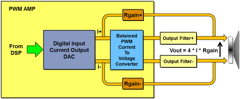
The synergy of the digital portion together with the amplification stage produces a system with optimised performance in terms of output noise and offset. In fact, unlike analog input amplifiers, which require a voltage gain typically > 20, the voltage gain of the output stage of the structure used in this system is 1. The digital input signal is converted into a current (equal to zero if the input signal is zero) that is the input of a current-to-voltage converter, with unity voltage gain. Generally speaking, lower voltage gain means less noise, offset and THD as shown in Figure 2.

Figure 2: Amplification stage of the Class D power amplifier
Precise diagnostics
The availability of the digitised output current value, together with the amplitude value of the digital input signal, allows dedicated algorithms inside the DSP to estimate the impedance of the load. The goal is to test the correct connection and some characteristics of the load, mainly for service purposes. But it can also be useful during normal device usage.
Moreover, the DSP is able to digitally generate internally a test tone in a precise way.
In currently available devices, the generation of a low frequency pulse to check the woofer and a tone at 20kHz to check the ‘open tweeter condition’ is included. In the next generation of power amplifiers, the internal DSP will be able to generate whatever test signal is required.
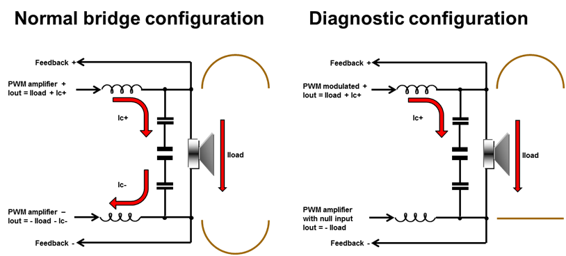
This kind of Class D power amplifier has interesting peculiarities. If we want to get precise information from the diagnostics with a signal next to 20kHz, the current flowing in the output filter capacitor can be an unacceptable error. Looking at Figure 3, we can see that in normal bridge configuration, the current in the channel (where the current sensor is present) is the sum of the load current Iload plus the error Ic-.

Figure 3: Diagnostics current in a bridge configuration
Without a signal in the negative half bridge, due to the feedback, the output is at a dc level too. No signal crosses the capacitor and Ic-, the error, is removed. Then, in the diagnostic configuration, the error in the current sensor is reduced.
Note that keeping the input signal at zero without feedback after the output filter is not enough to guarantee, at high frequency, Ic- = 0.
FDA4100LV and FDA450LV are the first ST Class D power amplifiers embedding all these features. The devices are built in a 0.6µm BCD technology, balancing cost and density.
ST is working on the development of this family with a more aggressive technology able to increase the logic density. Because of this, the goal of the next devices will be higher flexibility with better efficiency, taking advantage of the lower Rds-on per area of the power MOS available in recent technologies.


