How to deliver current beyond 100A to an ADAS processor
The electrification of vehicle systems is growing in advanced driver assistance systems (ADAS), which include vision analytics for autonomous driving, parking assistance, and adaptive control functions. Smart connectivity, safety-critical software applications, and neural network processing all require enhanced computing power in real time.
This article originally appeared in the Jan'24 magazine issue of Electronic Specifier Design – see ES's Magazine Archives for more featured publications.
By Canan Priess, Automotive Product Marketing Engineer, Texas Instruments
Meeting these advanced needs requires a multicore processor such as the TDA4VH-Q1, which can support electronic control units (ECUs) beyond 100 A. But the design challenges associated with high power include achieving efficiency for higher current rails, controlling thermal performance and load transients at full loads, and meeting functional safety requirements.
Delivering ADAS processing power
The TPS62876-Q1 buck converter helps designers address currents beyond 30A with a novel stackability feature that achieves the high currents necessary to power a system-on a-chip (SoC) such as the TDA4VH-Q1. The family includes devices ranging from 15 to 30A, available in the same package, and Stack features that can support load current beyond 100A.
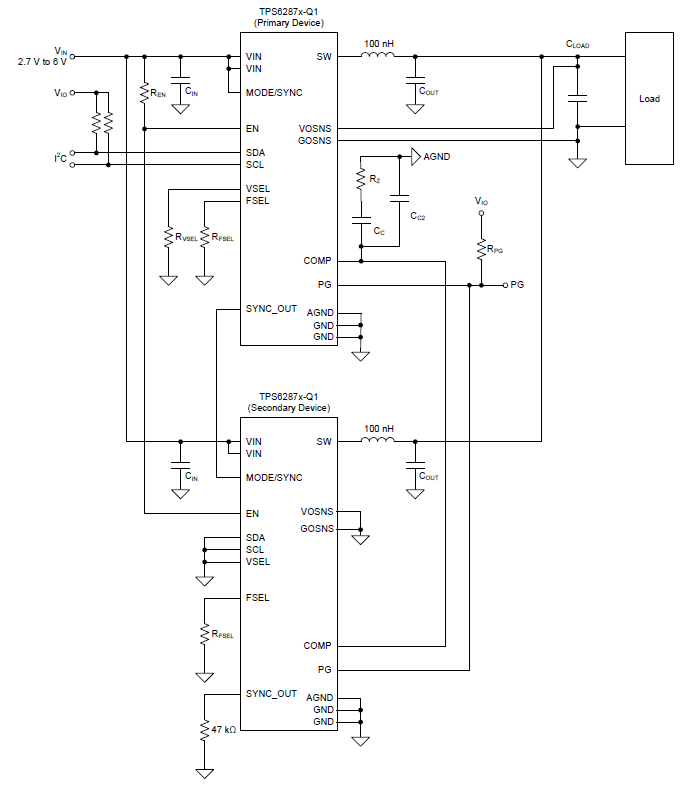
Stacking these devices not only helps power the core of next-generation ADAS SoCs, but also helps improve thermal performance by reducing thermal limitations and increase efficiency. See Figure 1.

Figure 1. Two TPS62876-Q1devices in a stacked configuration
Stacking operates by using the daisy-chain method. The primary device controls one compensation network, one POWERGOOD pin, one ENABLE pin, and one I2C interface. For optimal current sharing, you must program all devices in the stack to use the same current rating, the same switching frequency, and the same current level.
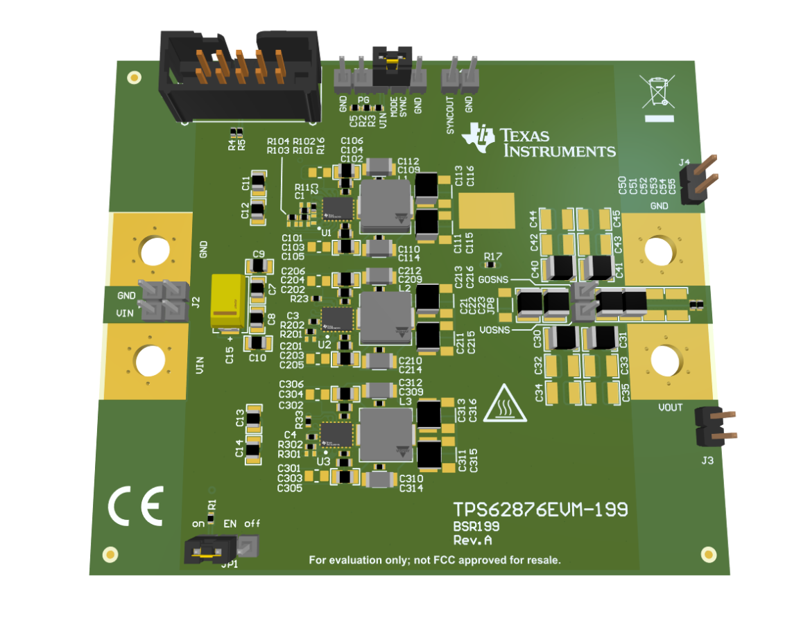
The primary device in the stack also sets the output voltage and controls its regulation. If there is a 47-kΩ resistor between the SYNCOUT pin and ground, the device operates as a secondary device. If the SYNCOUT pin is high impedance, the device operates as a primary device. Figure 2 shows the stack configuration implemented on a printed circuit board.

Figure 2. Example evaluation module of three stacked TPS62876-Q1 buck converter
Other features in this family of buck converters include:
Droop compensation, also known as load line (automatic voltage positioning). Scaling the nominal output voltage provides better load-transient tolerance based on the output current (15 to 30A) and helps reduce the output capacitance, enabling a cost-optimised, high-power-density solution. The REGISTER pin enables or disables droop compensation, which is disabled by default.
Remote sensing supports a wider range of SoC processors with a tighter output-voltage requirement that provides more headroom during load transients. The device’s remote sense lines connect directly to the point of load, which allows you to set the voltage with an accuracy of 0.8%.
The I2C interface monitors system performance and sends a warning if the temperature and output current exceed specified limits. It is also possible to use dynamic voltage scaling to adjust the output voltage from 0.4 to 1.675V. If you do not need the I2C feature, you can still use the same device by connecting the SCL and SDA pins to ground.
Functional safety
Functional safety is an important aspect in ADAS, especially when it comes to autonomous driving. The TPS62876-Q1 buck converter offers TI Functional Safety-Capable levels of documentation, which include:
- The functional safety failure-in-time rates of the semiconductor component estimated by the application of industry reliability standards
- Component failure modes and their distribution based on the device’s primary function
- Pin failure-mode analysis
- Adding an external supervisor to your design enables you to achieve Automotive Safety Integrity Level standards
Conclusion
Moving toward higher autonomy levels such as Society of Automotive Engineers Level 2 will require more computational capabilities to provide higher resolutions and quick responses in a very short time. Embedding features such as artificial intelligence technologies also increases the need for more power-hungry ADAS SoC processors. The stackability of the TPS62876-Q1 family helps you achieve core power beyond 100A to enable a higher level of autonomous driving.


