
Analysis
austriamicrosystems continuously expands CMOS, High-Voltage, High-Voltage Flash and RF Multi Project Wafer Services for Foundry Customers
austriamicrosystems' Full Service Foundry business unit today released its further expanded fast and cost-efficient ASIC prototyping service, known as Multi-Project Wafer (MPW) or shuttle run, with an even more extensive schedule in 2011. The service, which combines several designs from different customers onto one wafer offers significant cost advantages for foundry customers as the costs for wafer and masks are shared among a number of different shuttle participants.
austFor the 0.35µm specialty processes, which are based on the 0.35µm CMOS process transferred from TSMC (Taiwan Semiconductor Manufacturing Company) a total of 15 runs are offered in 2011. austriamicrosystems' 0.35µm High-Voltage CMOS process family with a 20V CMOS option, ideally suited for power management products and display drivers, a 50V CMOS process, optimized for automotive and industrial applications, and a 120V module optimized for sensor and sensor interface chips serve customers’ demand for high-voltage applications and products. The advanced High-Voltage CMOS process with Embedded Flash functionality adds to austriamicrosystems’ MPW service portfolio. The CMOS compatible 0.35µm Silicon-Germanium BiCMOS technology S35 enables RF circuit designs with an operating frequency of up to 6 GHz combined with high-density digital parts on one single ASIC.
Overall austriamicrosystems will offer almost 150 MPW start dates in 2011, enabled by long lasting co-operations with organizations such as CMP-TIMA, Europractice, Fraunhofer IIS, and Mosis. The complete schedule for 2011 has now been released and detailed start dates per process are available on the web at http://asic.austriamicrosystems.com/MPW.
To take advantage of the MPW service, austriamicrosystems’ foundry customers deliver their completed GDSII-data at specific dates and receive untested packaged samples or dies within a short lead-time of typically 8 weeks for CMOS and 10 weeks for 0.35µm High-Voltage CMOS, SiGe-BiCMOS and Embedded Flash processes. All 0.35µm MPW runs will be produced at austriamicrosystems’ state-of-the-art 8 inch wafer fab in Austria.
All process technologies are supported by the well-known HIT-Kit, an industry benchmark process design kit based on Cadence, Mentor Graphics or Agilent ADS design environments. The HIT-Kit comes complete with fully silicon-qualified standard cells, periphery cells and general purpose analog cells such as comparators, operational amplifiers, low power A/D and D/A converters. Custom analog and RF devices, physical verification rule sets for Assura and Calibre as well as excellently characterized circuit simulation models enable rapid design starts of complex high performance mixed-signal ICs. In addition to standard prototype services, austriamicrosystems also offers analog IP blocks, a memory (RAM/ROM) generation service and packaging services in ceramic or plastic.
Product Spotlight
TBF10SL-4PS-B
ITT Interconnect Solutions

Circular Connector Standard 5/2 Female Sockets/Male Pins Panel Mount
CA/5015 Co...
| SKU: | TBF10SL-4PSB-ND |
|---|---|
| Stock: | 0 |
| Cost: | $45.59 |
CAA572C0G3A663J640LJ
TDK Corporation

Speciality Ceramic Capacitors Inline MEGA Cap,2220,C0G,1000V,66nF,+/-5%,6.4mm AE...
| SKU: | |
|---|---|
| Stock: | 1037 |
| Cost: | $9.16 |
RA1113112R
E-Switch, Inc.
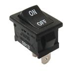
E-Switch / RS PRO RA1113112R Rocker Switch, SPST, OFF-ON, 10A, 125V AC, QC 0.187...
| SKU: | EG5619-ND |
|---|---|
| Stock: | 5586 |
| Cost: | $0.55 |
R30-3002002
Harwin

20.00mm M3 Metric M/F Threaded Hex Brass Spacer/Pillar
Hardware - Spacer (Stand...
| SKU: | |
|---|---|
| Stock: | 6545 |
| Cost: | $0.76 |
NRF54L15-QFAA-R
Nordic Semiconductor

RF System on a Chip - SoC Ultra-low power Bluetooth Multiprotocol 5.4 SoC System...
| SKU: | 4823-NRF54L15-QFAA-RTR-ND |
|---|---|
| Stock: | 0 |
| Cost: | $2.39 |
STDRIVEG611Q
STMicroelectronics

Gate Drivers High voltage and high-speed half-bridge gate driver for GaN power s...
| SKU: | 497-STDRIVEG611QTR-ND |
|---|---|
| Stock: | 0 |
| Cost: | $2.63 |
TBF10SL-4PS-B
ITT Interconnect Solutions
Circular Connector Standard 5/2 Female Sockets/Male Pins Panel Mount
CA/5015 Co...
| SKU: | TBF10SL-4PSB-ND |
|---|---|
| Stock: | 0 |
| Cost: | $45.59 |
CAA572C0G3A663J640LJ
TDK Corporation
Speciality Ceramic Capacitors Inline MEGA Cap,2220,C0G,1000V,66nF,+/-5%,6.4mm AE...
| SKU: | |
|---|---|
| Stock: | 1037 |
| Cost: | $9.16 |
RA1113112R
E-Switch, Inc.
E-Switch / RS PRO RA1113112R Rocker Switch, SPST, OFF-ON, 10A, 125V AC, QC 0.187...
| SKU: | EG5619-ND |
|---|---|
| Stock: | 5586 |
| Cost: | $0.55 |
R30-3002002
Harwin
20.00mm M3 Metric M/F Threaded Hex Brass Spacer/Pillar
Hardware - Spacer (Stand...
| SKU: | |
|---|---|
| Stock: | 6545 |
| Cost: | $0.76 |
NRF54L15-QFAA-R
Nordic Semiconductor
RF System on a Chip - SoC Ultra-low power Bluetooth Multiprotocol 5.4 SoC System...
| SKU: | 4823-NRF54L15-QFAA-RTR-ND |
|---|---|
| Stock: | 0 |
| Cost: | $2.39 |
STDRIVEG611Q
STMicroelectronics
Gate Drivers High voltage and high-speed half-bridge gate driver for GaN power s...
| SKU: | 497-STDRIVEG611QTR-ND |
|---|---|
| Stock: | 0 |
| Cost: | $2.63 |